
Appearance
AXRF49 User Manual

Alinx Electronic Limited
Company Website: www.en.alinx.com
Service Hotline: +86 21 67676997
Technical Support : technical@alinx.com
Document Information
| Item | Content |
| Document Name | Product Manual |
| Product Model | AXRF49 |
| Document Version | V1.0 |
| Prepared by | Alinx Electronic Limited |
| Release Date | 2026.9.23 |
Document Revision History
| Version | Date | Section | Revision Summary |
| V1.0 | 2026.9.23 | All | Initial Release |
The AXRF49 development board consists of an ACRF49 SoM and a carrier board, which are interconnected via a high-speed board-to-board connector.
The ACRF49 SoM is powered by the Xilinx Zynq UltraScale+ RFSoC Gen3 ZU49DR FPGA. It supports 16 channels of 14-bit RF-ADC with a maximum sampling rate of 2.5 GSPS, and 16 channels of 14-bit RF-DAC with a maximum sampling rate of 9.85 GSPS. By integrating high-performance ADC and DAC resources directly into the FPGA, the platform significantly reduces the complexity of the RF signal processing chain, maximizes input/output channel density without compromising bandwidth, and achieves lower overall power consumption through the elimination of external ADC/DAC components and associated interface power dissipation. The Zynq UltraScale+ RFSoC integrates an ARM Cortex-A53 processing system, UltraScale+ programmable logic, and industry-leading signal processing bandwidth, delivering a fully integrated RF signal chain suitable for applications such as wireless communications, cable TV access, test and measurement, early warning and radar systems, and other high-performance RF systems.
The ACRF49 SoM is equipped with ten Micron DDR4 memory devices (MT40A512M16LY). Five devices are connected to the PS side, forming a 64-bit data bus with ECC support, while the remaining five devices are connected to the PL side, forming a 72-bit data bus. In addition, the SoM integrates a 1 Gb QSPI Flash and an 8 GB eMMC device for system boot configuration and storage of system files.
The carrier board provides a comprehensive set of peripheral interfaces for the SoM, including one M.2 NVMe interface, one USB 3.0 interface, one Gigabit Ethernet interface, one JTAG/UART interface, one TF card interface, one FMC+ expansion interface, and two QSFP28 interfaces.The image below shows the actual appearance of the development board.
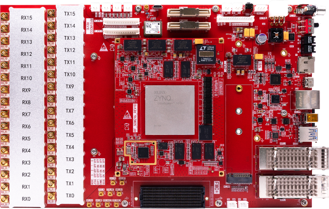
Figure 1 - development board
Note: Depending on the hardware version and configuration, the appearance of this module may differ slightly from that shown in this document.
Part 1:FPGA Development Board Introduction
Figure 1.1.1 below illustrates the schematic diagram of the overall development system.
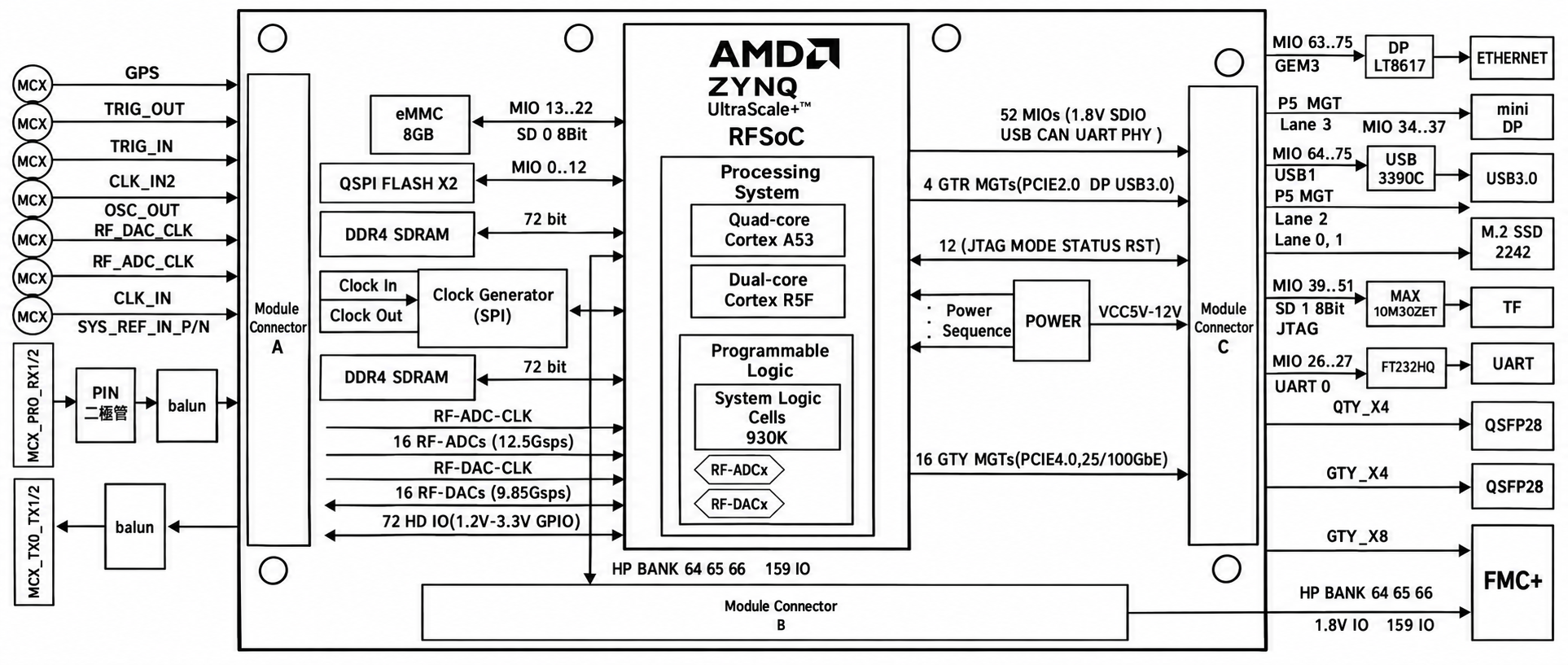
Figure1.1.1 - The Schematic Diagram of the AXRF49
From this diagram, you can clearly identify the interfaces and functions supported by the AXRF49 development platform.
ACRF49 SoM: The module integrates a ZU49DR device, 4GB DDR4 (PS), 4GB DDR4 (PL), 1Gb QSPI Flash, and 8GB eMMC. It also provides two onboard crystal oscillator clock sources: a 33.3333 MHz single-ended active oscillator for the PS system, and a 32.76 kHz crystal oscillator used to drive the RFSoC’s internal RTC circuit.
M.2 Interface: One PCIe x2 standard M.2 interface for connecting an M.2 SSD solid-state drive.
USB 3.0 Interface: One USB3.0 interface supporting HOST, SLAVE, and three modes.
Gigabit Ethernet Interface: One 10M/100M/1000M Ethernet RJ45 interface, used for Ethernet data exchange with computers or other network devices.
JTAG & UART interface: The JTAG&UART debug interface uses a Type-C connector, with JTAG and UART sharing this interface for FPGA program download and debugging.
Micro SD Card Socket: One Micro SD card socket for storing operating system images and file systems.
FMC+ Expansion Interface: One FMC+ expansion interface for adding other FMC daughter cards.
QSFP28 Optical Fiber Interface: Two QSFP28 optical fiber interfaces supporting communication rates of 40G/100G.
Expansion IO:Three groups of expansion IO, two groups of PL-side expansion IO and one group of PS-side expansion IO, available for user-defined use.
LED Indicator: Four expandable LED through-hole sockets for user-defined applications.
Board-to-Board and Mezzanine Connector: Two 80-pin 5mm board-to-board and mezzanine connectors.
Button: One reset button.
Part 2:ACRF49 SoM
2.1 ACRF49 SoM Introduction
The Zynq chip on the ACRF49 SoM is based on Xilinx's Zynq UltraScale+ RFSoC Gen3 series ZU49DR-2FSVF1760I.
The ACRF49 SoM is equipped with ten Micron DDR4 chips (MT40A512M16). Five DDR4 chips are connected to the PS side, forming a 64-bit data bus with ECC support, while the remaining five DDR4 chips are connected to the PL side, forming a 72-bit data bus. Each DDR4 chip has a capacity of 1 GB. The maximum operating frequency of the DDR4 SDRAM is up to 1333 MHz (corresponding to a data rate of 2666 Mbps). In addition, the SoM integrates a 1 Gbit QSPI Flash for boot configuration and system file storage.
To interface with the carrier board, the ACRF49 SoM features three 800-pin high-speed board-to-board connectors. These connectors provide access to PS-side interfaces including USB 3.0, Gigabit Ethernet, SD card, M.2, DisplayPort (DP), and the remaining MIO signals, as well as PL-side interfaces including two QSFP28 ports, one FMC+ expansion interface, and additional user expansion I/O signals.
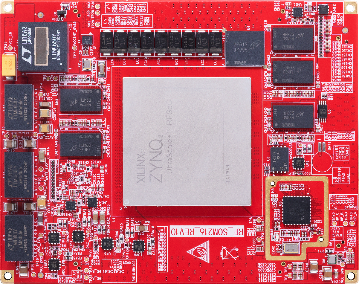
Figure2.1.1-ACRF49 SoM (Front View)
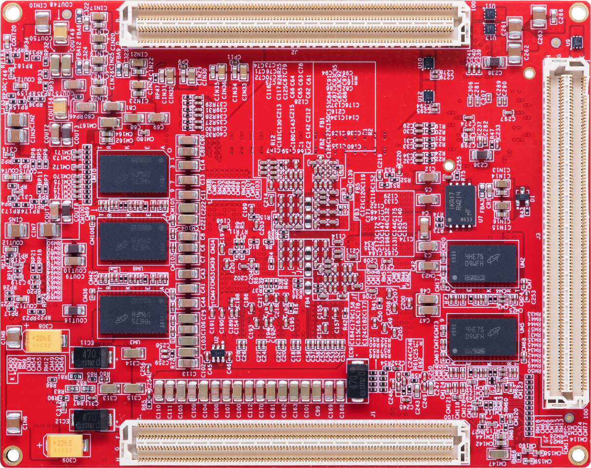
Figure2.1.2-ACRF49 SoM (Back View)
2.2 MPSOC Chip
The ACRF49 SoM is based on the Xilinx Zynq UltraScale+ RFSoC Gen3 series chip, model ZU49DR-2FSVF1760I. The programmable logic (PL) section provides abundant FPGA resources for high-throughput digital signal processing (DSP) and supports a wide range of IP cores, including digital up/down conversion (DUC/DDC) kernels. FPGA acceleration can be efficiently implemented through software-defined radio (SDR) development frameworks, application programming interfaces (APIs), and FPGA infrastructure, enabling rapid system development and allowing users to focus on value-added IP design. Pre-validated FPGA functions such as Fast Fourier Transform (FFT) and Finite Impulse Response (FIR) filters provide an excellent starting point, while custom IP blocks can be seamlessly integrated into the modular architecture using the user’s preferred hardware description language (HDL).
In addition to the FPGA fabric, the Xilinx UltraScale+ RFSoC integrates four application processing units (APUs) and two real-time processing units (RPUs), making it well suited for applications that require an embedded operating system and independent system operation.
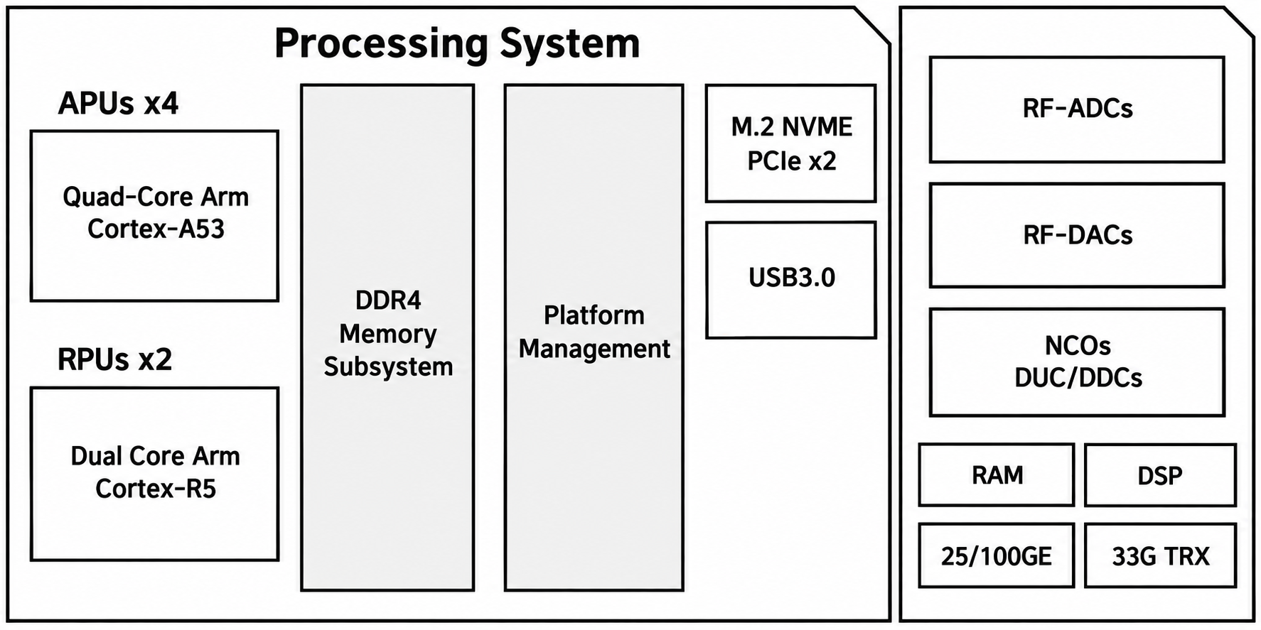
Figure2.2.1- RFSOM Hardware System Block Diagram
2.3 DDR4 DRAM
The ACRF49 SoM is equipped with ten Micron 1 GB DDR4 chips, model MT40A512M16LY-075E. Five DDR4 chips are connected to the PS side, forming a 64-bit data bus with ECC support, while the remaining five DDR4 chips are connected to the PL side, forming a 72-bit data bus.
The PS-side DDR4 SDRAM operates at a maximum clock frequency of 1200 MHz (data rate of 2400 Mbps), with the five DDR4 memory chips directly interfaced to the PS BANK 504 memory controller. The PL-side DDR4 SDRAM operates at a maximum clock frequency of 1333 MHz (data rate of 2666 Mbps), with the five DDR4 chips connected to the FPGA BANKs 67, 68, and 69.
The detailed configurations of the PS-side and PL-side DDR4 SDRAM are summarized in Table 2.3.1.
| Position | Reference | Part number | Form | Factory |
| PS | UM1,UM2,UM5,UM6,UM9 | MT40A512M16LY-075E | 512x16bit | Micron |
| PL | UM3,UM4,UM7,UM8,UM10 | MT40A512M16LY-075E | 512x16bit | Micron |
Table2.3.1- DDR4 SDRAM Configuration
The hardware connection method for the PS-side DDR4 is shown in Figure 2.3.1:
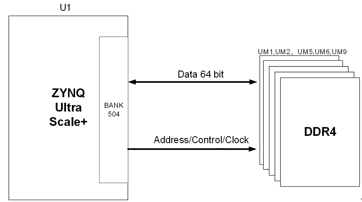
Figure 2.3.1-PS DDR4 DRAM block diagram
The hardware connection method for the PL-side DDR4 SDRAM is shown in Figure 2.3.2:
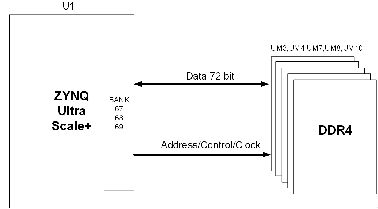
Figure2.3.2-PL DDR4 DRAM block diagram
2.4 QSPI Flash
The ACRF49 SoM integrates two 512 Mbit Quad-SPI (QSPI) Flash chips, forming an 8-bit data bus. The Flash device model is MT25QU512ABBIEW9-0SIT and operates at a 1.8 V CMOS voltage standard. Due to the non-volatile nature of QSPI Flash memory, it can be used as the system boot device for storing boot images. These images primarily include FPGA configuration bitstreams, ARM application code, and user data files. The detailed model information and key characteristics of the QSPI Flash are listed in Table 2.4.1.
| Position | Reference | Part number | Capacity | Factory |
| PS | U6,U7 | MT25QU512ABBIEW9-0SIT | 512Mbit | Micron |
Table 2.4.1- QSPI FLASH Specification
The QSPI FLASH is connected to the MIO of BANK500 on the ZYNQ chip's PS side. In system design, these MIO functions on the PS side need to be configured as QSPI FLASH interfaces.
Figure2.4.1 shows the QSPI Flash in the schematic.
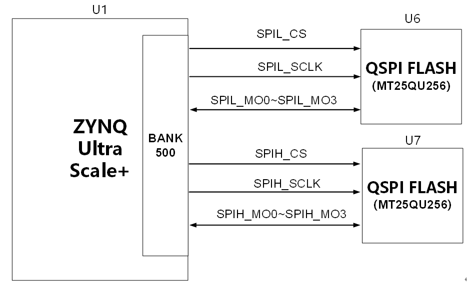
Figure2.4.1- QSPI Flash in the schematic
Configure chip pin assignments:
| Signal Name | Pin Name | Pin Number |
| SPIL_SCLK | PS_MIO0 | BB27 |
| SPIL_MO1 | PS_MIO1 | BA27 |
| SPIL_MO2 | PS_MIO2 | BB26 |
| SPIL_MO3 | PS_MIO3 | BB28 |
| SPIL_MO0 | PS_MIO4 | BA28 |
| SPIL_CS | PS_MIO5 | BA29 |
| SPIH_CS | PS_MIO7 | AY27 |
| SPIH_MO0 | PS_MIO8 | AW27 |
| SPIH_MO1 | PS_MIO9 | AW26 |
| SPIH_MO2 | PS_MIO10 | AV26 |
| SPIH_MO3 | PS_MIO11 | AW28 |
| SPIH_SCLK | PS_MIO12 | AV28 |
Table 2.4.2- QSPI Flash chip pin assignment
2.5 eMMC Flash
The ACRF49 SoM is equipped with one 8 GB eMMC Flash chip, model MTFC8GLVEA-1MWT, supporting a 1.8 V voltage standard. The data bus width between the eMMC Flash and the Zynq chip is 8 bits. Owing to its large capacity and non-volatile nature, the eMMC Flash serves as a high-capacity storage device within the Zynq system and is typically used to store ARM application programs, system files, and other user data. The specific model information and related parameters of the eMMC Flash are listed in Table 2.5.1.
| Position | Reference | Part Number | Capacity | Factory |
| PS | U8 | MTFC8GLVEA-1MWT | 8G Byte | Micron |
Table 2.5.1-eMMC FLASH Specification
The eMMC Flash is connected to the MIO pins of BANK 500 on the Zynq PS side. In system design, these PS-side MIO pins must be configured to function as eMMC interfaces. The connection of the eMMC Flash in the schematic diagram is shown in Figure 2.5.1.
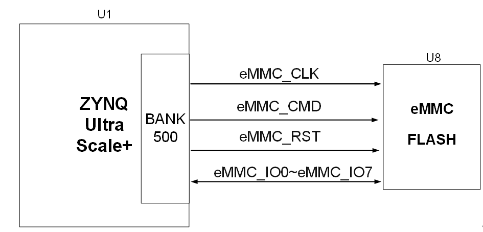
Figure2.5.1- eMMC Flash in the schematic
Configuration Chip Pin assignment:
| Signal Name | Pin Name | Pin Number |
| EMMC_RST | PS_MIO23 | AM27 |
| EMMC_CLK | PS_MIO22 | AL27 |
| EMMC_CMD | PS_MIO21 | AN28 |
| EMMC_IO0 | PS_MIO13 | AU26 |
| EMMC_IO1 | PS_MIO14 | AU27 |
| EMMC_IO2 | PS_MIO15 | AT27 |
| EMMC_IO3 | PS_MIO16 | AU28 |
| EMMC_IO4 | PS_MIO17 | AT28 |
| EMMC_IO5 | PS_MIO18 | AP28 |
| EMMC_IO6 | PS_MIO19 | AR27 |
| EMMC_IO7 | PS_MIO20 | AP27 |
Table2.5.2-eMMC Flash Pin Configuration
2.6 EEPROM
The ACRF49 SoM includes a built-in EEPROM chip, model AT24CM01, with a capacity of 1 Mbit. It is connected to the PS side via an I2C bus for communication.
EEPROM Pin Assignment:
| Signal Name | Pin Name | Pin Number | Remarks |
| IIC_SCL | PS_MIO24 | AL28 | I2C Clock Signal |
| IIC_SDA | PS_MIO25 | AM28 | I2C Data Signal |
Table2.6.1- EEPROM Pin Assignment
2.7 Clock configuration
The ACRF49 SoM provides dual crystal oscillators for system clock generation. The main system clock is supplied by a 33.3333 MHz active crystal oscillator in a 3.2 x 2.5 mm package. In addition, a 32.768 kHz crystal oscillator is used to drive the RFSoC’s internal real-time clock (RTC) circuit. The schematic diagram of the clock circuit design is shown in Figure 2.7.1.
The ACRF49 SoM employs the LMK04828 clock distribution chip to generate and distribute the clocks required by the ADC and DAC modules. The primary reference source is 96 MHz high-stability VCXO. The system supports both a single-ended external reference clock input and a differential SYSREF input, enabling multiple modules to be synchronized in parallel to form large-scale coherent RF channels.
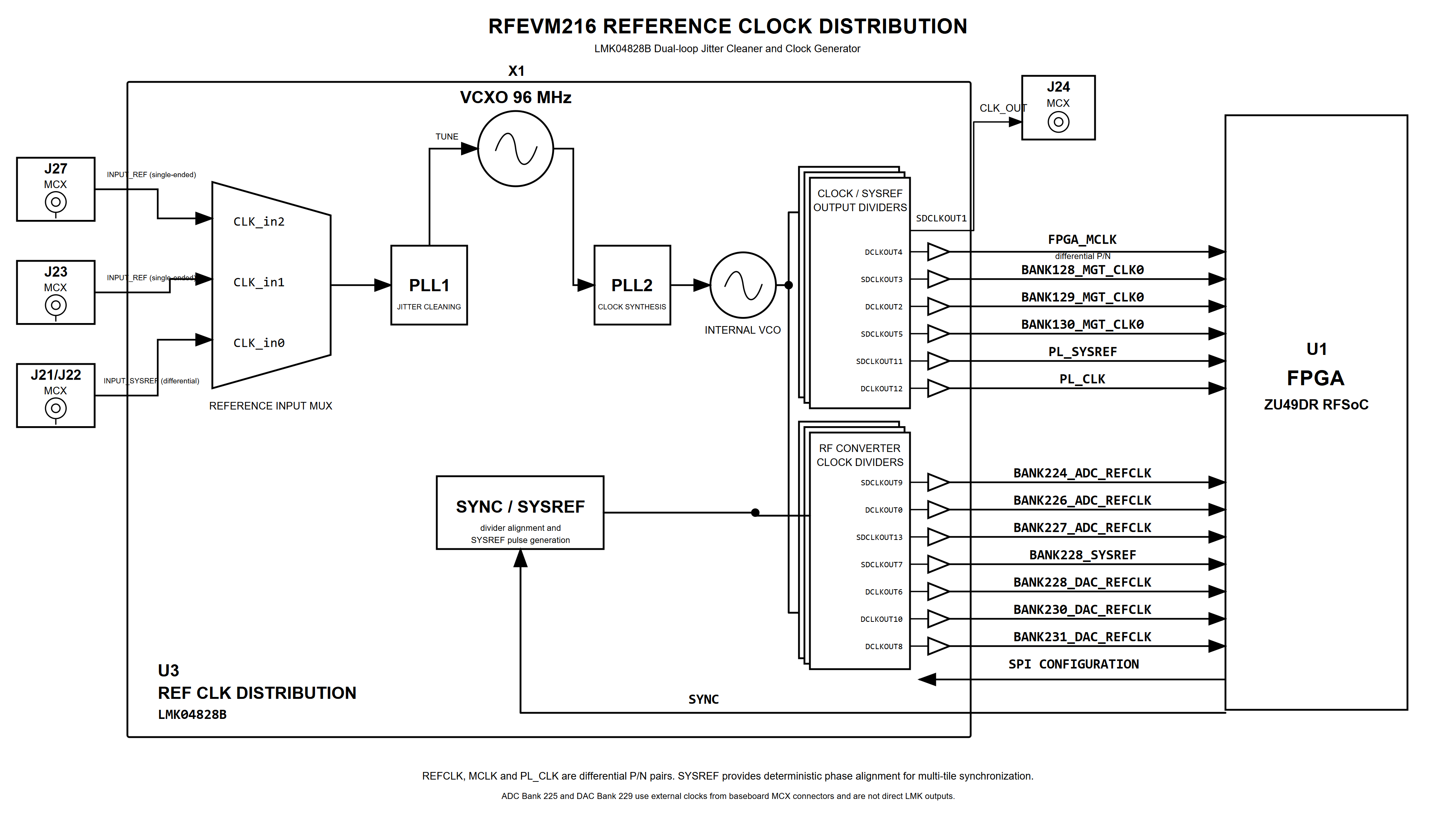
Figure2.7.1- Clock Distribution Connection Schematic
2.8 RF-ADC Interface
The FPGA chip used on the ACRF49 SoM belongs to the Xilinx Zynq UltraScale+ RFSoC Gen3 series, which is the industry’s only single-chip adaptive radio platform. This chip integrates 14-bit RF-ADC channels with a maximum sampling rate of up to 2.5 GSPS, and the corresponding VCM signals are also routed to the board connector for external access.
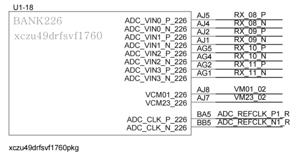
Figure2.8.1- RF-ADC Interface Schematic
2.9 RF-DAC Interface
The FPGA chip used on the ACRF49 SoM belongs to the Xilinx Zynq UltraScale+ RFSoC Gen3 series, the industry’s only single-chip adaptive radio platform. This chip integrates 14-bit RF-DAC channels with a maximum sampling rate of up to 9.85 GSPS.
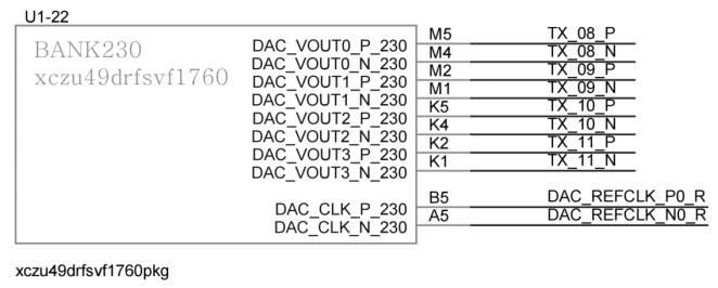
Figure2.9.1- RF-DAC Interface Schematic
2.10 High-Speed Board-to-Board Connector
The ACRF49 SoM provides three high-speed expansion interfaces, which are connected to the carrier board via three 400-pin board-to-board connectors (J1, J2, and J3). These connectors use Samtec’s ASP_230332-01 series devices with a 0.635 mm pitch and a mating height of 5 mm, supporting data rates of up to 32 Gbps per channel.
2.11 Power Supply
The ACRF49 SoM is powered by a 12 V DC supply, which is delivered to the SoM through the carrier board via board-to-board connectors. The 12 V system power is converted into multiple voltage rails by high-efficiency step-down (buck) regulators to supply the FPGA and other onboard circuits. The power supplies for the ADC and DAC sections are generated by low-noise linear LDO regulators, providing excellent power supply rejection ratio (PSRR) to ensure high signal integrity and stable performance. The corresponding voltage levels of the SoM expansion I/O BANK interfaces are illustrated in Table 2.11.1.
| BANK | Level (V) | Remarks |
| BANK64 | Provided from baseboard, 1.8V | HP BANK |
| BANK65 | Provided from baseboard, 1.8V | HP BANK |
| BANK66 | Provided from baseboard, 1.8V | HP BANK |
| BANK67 | Fixed at 1.2V | DDR4 signals |
| BANK68 | Fixed at 1.2V | DDR4 signals |
| BANK69 | Fixed at 1.2V | DDR4 Signal |
| BANK84 | 1.8V Fixed | LMK04828 Configuration Signal and Output |
| BANK87 | Provided from Baseboard, 3.3V | HD BANK |
| BANK88 | Provided from Baseboard, 3.3V | HD BANK |
| BANK89 | Provided from Baseboard, 3.3V | HD BANK |
| BANK128 | MGTY | FMC+ Signal |
| BANK129 | MGTY | FMC+ Signal |
| BANK130 | MGTY | QSFP28 Signal |
| BANK131 | MGTY | QSFP28 Signal |
| BANK500 | 1.8V Fixed | QSPI and EMMC Signal |
| BANK501 | Provided from Baseboard | MIO BANK supports 1.8V, 2.5V, and 3.3V at ±5% |
| BANK502 | Provided from Baseboard | MIO BANK supports 1.8V, 2.5V, and 3.3V at ±5% |
| BANK503 | Provided from Baseboard | MIO BANK supports 1.8V, 2.5V, and 3.3V at ±5% |
| BANK505 | PS_MGTR | All high-speed signal pins and clock signals are routed out to the connector |
Table 2.11.1- Voltage levels
The power design block diagram of the SoM is shown below:
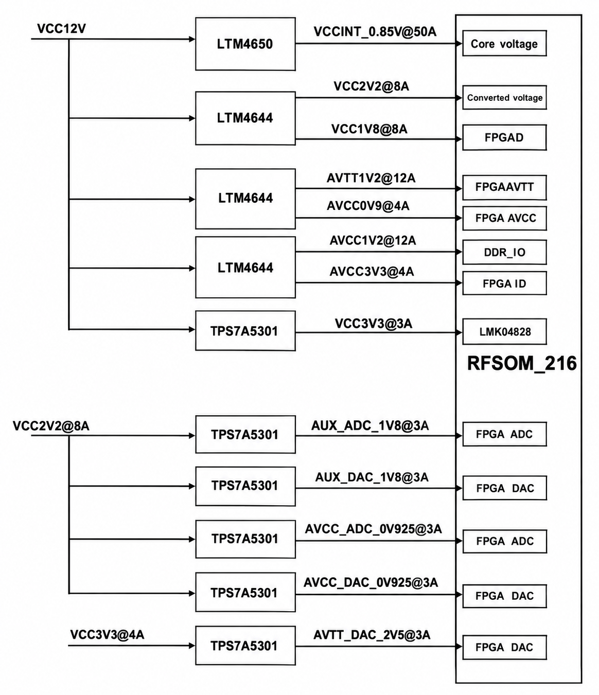
Figure2.11.1- Power Design Block Diagram
2.12 Structure Diagram
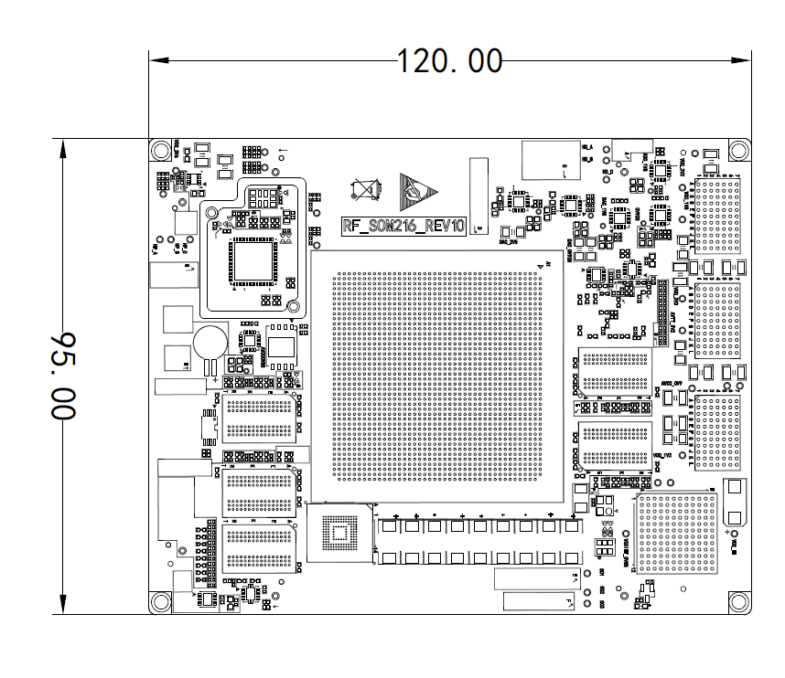
Figure2.12.1- Front View of ACRF49 SoM
Part 3:Carrier Board
3.1 Carrier Board Introduction
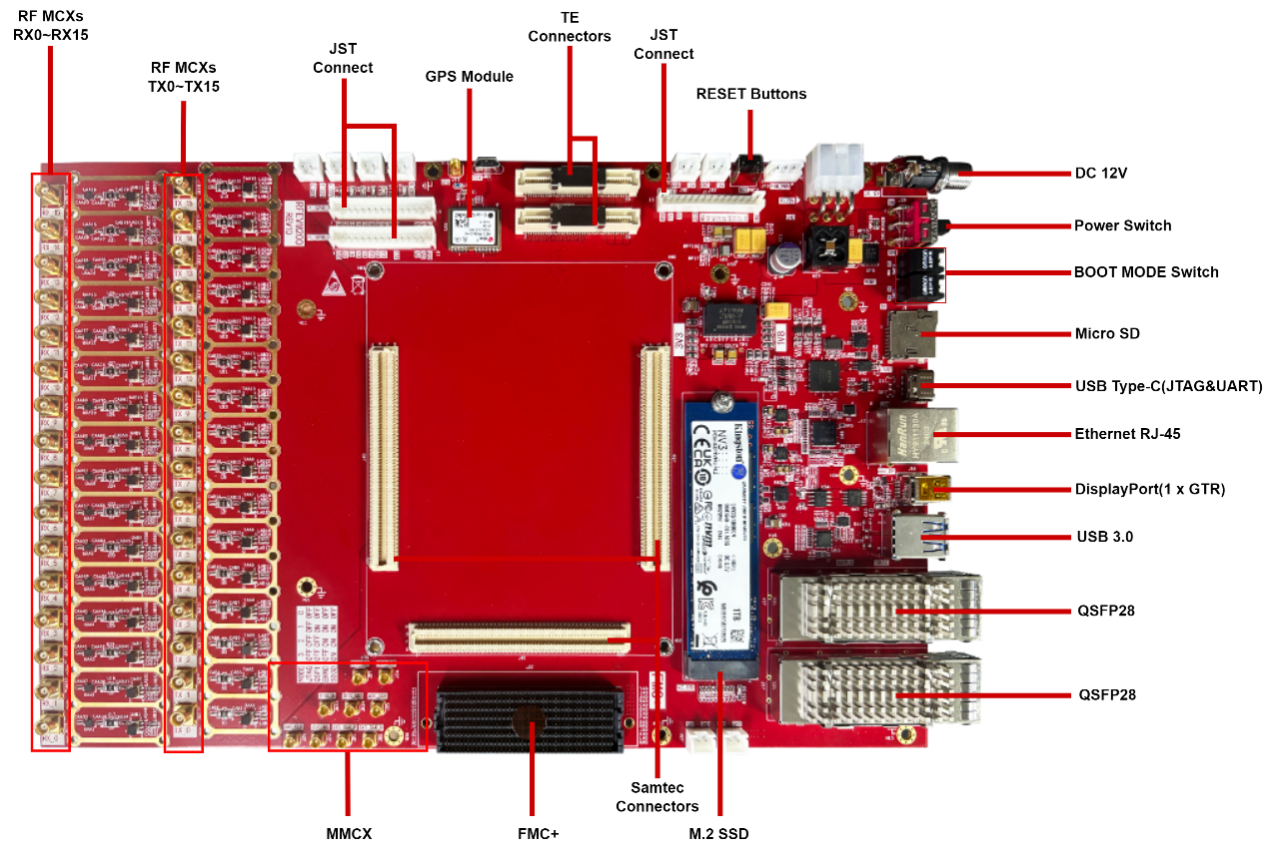
Figure3.1.1- Front View of Carrier Board
From the previous functional description, we can understand some of the carrier board's functions:
1x M.2 Interface
1x USB3.0 Interface
1x Gigabit Ethernet Interface
1x Type-C Interface for JTAG & UART
1x Micro SD Card Socket
1x DP Interface
2x QSFP28 Optical Ports
2 sets of PL Expansion IO x8, 1 set of PS Expansion IO
4 User LED Lights
1x FMC+ Expansion Interface
3.2 M.2 Interface
The AXRF49 carrier board is equipped with a PCIe x2 standard M.2 interface for connecting an M.2 SSD. The M.2 interface uses an M-key slot and supports PCIe only, not SATA. Therefore, users must choose a PCIe-based SSD when selecting a solid-state drive.
The PCIe signals are directly connected to the BANK505 PS MGT transceivers of the ZU47DR. Both TX and RX signals are routed as differential pairs to LANE0 and LANE1 of the MGT. The PCIe clock is supplied by a 100 MHz differential clock source. The schematic design of the M.2 circuit is shown in Figure 3.2.1:
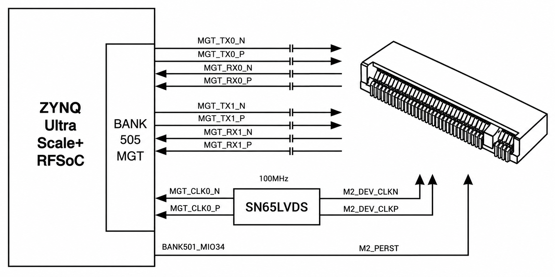
Figure 3.2.1- Schematic Design of M.2 Interface
Pin Assignment for M.2 Interface:
| Signal Name | ZYNQ Pin Number | M.2 Connector J19 | |
| Pin Number | Name | ||
| MGT_TX0_N | AH36 | 47 | PETn0 |
| MGT_TX0_P | AH35 | 49 | PETp0 |
| MGT_TX1_N | AG38 | 35 | PETn1 |
| MGT_TX1_P | AG37 | 37 | PETp1 |
| MGT_RX0_N | AJ42 | 41 | PERn0 |
| MGT_RX0_P | AJ41 | 43 | PERp0 |
| MGT_RX1_N | AH40 | 29 | PERn1 |
| MGT_RX1_P | AH39 | 31 | PERp1 |
| MGT_CLK0_N | AF35 | ||
| MGT_CLK0_P | AF34 | ||
Table 3.2.1- M.2 Interface Pin Assignment
3.3 USB3.0 Interface
The AXRF49 carrier board provides a USB 3.0 interface that supports both HOST and SLAVE modes, with data transfer rates of up to 5.0 Gb/s. The USB 3.0 signals are routed directly to the external Type-A connector. For USB 2.0 functionality, the ULPI interface is connected to an external USB3320C chip to enable high-speed USB 3.0 and USB 2.0 data communication. The USB 3.0 connection schematic is shown in Figure 3.3.1:
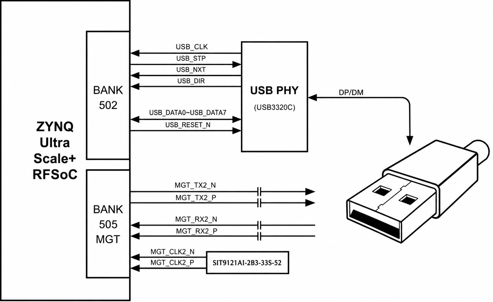
Figure 3.3.1: USB3.0 Interface Schematic
The pin assignments of USB 3.0 interface are as follows:
| Signal Name | Pin Name | ZYNQ Pin Number | Description |
| USB_TX_N | BANK505_MGT_TX2_N | AF40 | USB3.0 Data Transmit Negative |
| USB_TX_P | BANK505_MGT_TX2_P | AF39 | USB3.0 Data Transmit Positive |
| USB_RX_N | BANK505_MGT_RX2_N | AG42 | USB3.0 Data Receive Negative |
| USB_RX_P | BANK505_MGT_RX2_P | AG41 | USB3.0 Data Receive Positive |
| USB_DATA0 | BANK502_PS_MIO56 | N29 | USB2.0 Data Bit0 |
| USB_DATA1 | BANK502_PS_MIO57 | R29 | USB2.0 Data Bit1 |
| USB_DATA2 | BANK502_PS_MIO54 | N28 | USB2.0 Data Bit2 |
| USB_DATA3 | BANK502_PS_MIO59 | T30 | USB2.0 Data Bit3 |
| USB_DATA4 | BANK502_PS_MIO60 | U28 | USB2.0 Data Bit4 |
| USB_DATA5 | BANK502_PS_MIO61 | T28 | USB2.0 Data Bit5 |
| USB_DATA6 | BANK502_PS_MIO62 | V28 | USB2.0 Data Bit6 |
| USB_DATA7 | BANK502_PS_MIO63 | T29 | USB2.0 Data Bit7 |
| USB_STP | BANK502_PS_MIO58 | R30 | USB2.0 Stop Signal |
| USB_DIR | BANK502_PS_MIO53 | N30 | USB2.0 Data Direction Signal |
| USB_CLK | BANK502_PS_MIO52 | P28 | USB2.0 Clock Signal |
| USB_NXT | BANK502_PS_MIO55 | P29 | USB2.0 Next Data Signal |
| USB_RESET_N | BANK501_PS_MIO35 | C33 | USB2.0 Reset Signal |
Table 3.3.1- USB 3.0 Pin Configuration
3.4 Gigabit Ethernet Interface
The AXRF49 carrier board includes a Gigabit Ethernet interface connected to the PS side. It uses the TI DP83867ISR Ethernet PHY to provide reliable network communication. The PS-side Ethernet PHY is interfaced with the ZYNQ PS MIO pins on BANK502. The DP83867 supports 10/100/1000 Mbps data rates and communicates with the ZYNQ system’s MAC layer through an RGMII interface. The schematic diagram of the Gigabit Ethernet PHY connection is shown below:
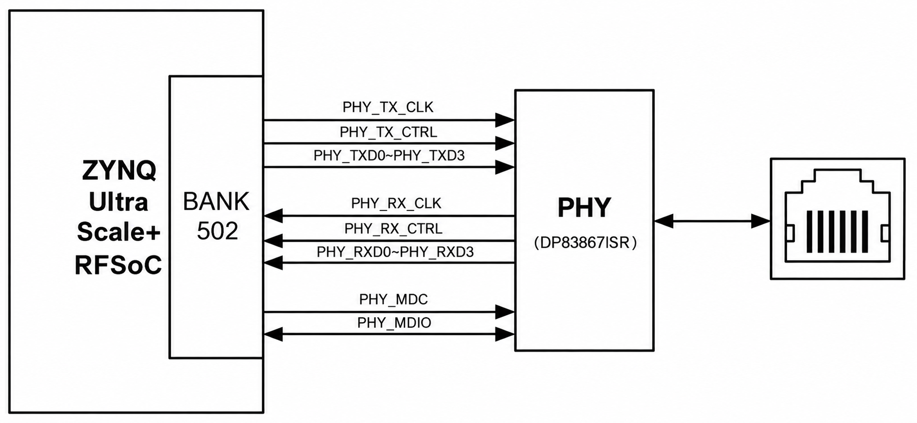
Figure 3.4.1- Ethernet Connection Schematic
DP83867ISR PHY Connection to XCZU49DR RFSoC:
| Signal Name | Pin Number | Pin Number | DP83867 PHY U48 | |
| Pin Number | Pin Name | |||
| PHY_TX_CLK | BANK502_PS_MIO64 | U30 | 29 | GTX_CLK |
| PHY_TXD0 | BANK502_PS_MIO65 | V30 | 28 | TX_D0 |
| PHY_TXD1 | BANK502_PS_MIO66 | V29 | 27 | TX_D1 |
| PHY_TXD2 | BANK502_PS_MIO67 | W28 | 26 | TX_D2 |
| PHY_TXD3 | BANK502_PS_MIO68 | Y29 | 25 | TX_D3 |
| PHY_TX_CTRL | BANK502_PS_MIO69 | W29 | 37 | TX_CTRL |
| PHY_RX_CLK | BANK502_PS_MIO70 | AA28 | 32 | RX_CLK |
| PHY_RXD0 | BANK502_PS_MIO71 | AB28 | 33 | RX_D0 |
| PHY_RXD1 | BANK502_PS_MIO72 | AC28 | 34 | RX_D1 |
| PHY_RXD2 | BANK502_PS_MIO73 | AA29 | 35 | RX_D2 |
| PHY_RXD3 | BANK502_PS_MIO74 | Y30 | 36 | RX_D3 |
| PHY_RX_CTRL | BANK502_PS_MIO75 | AC29 | 38 | RX_CTRL |
| PHY_MDC | BANK502_PS_MIO76 | AB30 | 16 | MDC |
| PHY_MDIO | BANK502_PS_MIO77 | AA30 | 17 | MDIO |
| PS_POR_B | BANK501_PS_MIO26 | A34 | 43 | RESET_N |
Table 3.4.1- Gigabit Ethernet Interface Pin Assignment
3.5 Micro SD Card Socket
The AXRF49 carrier board provides a Micro SD card interface for convenient access to SD card storage. It can be used to store the BOOT program, Linux operating system kernel, file system, and other user data files.
The SD card I/O signals are connected to the MIO pins of PS BANK501. The schematic diagram of the SD card connection to the PS is shown in Figure 3.5.1.
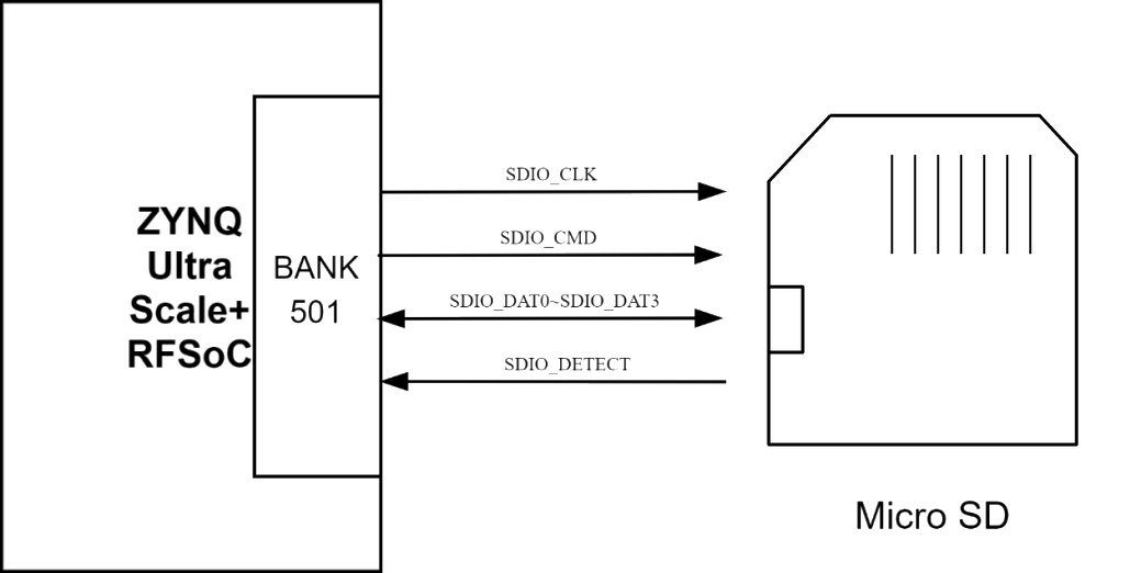
Figure3.5.1- SD Card Connection Schematic
SD Card Pin Assignment:
| Signal Name | Pin Name | Pin Number | Description |
| SDIO_CLK | BANK501_PS_MIO51 | M31 | SD Clock Signal |
| SDIO_CMD | BANK501_PS_MIO50 | M30 | SD Command Signal |
| SDIO_DAT0 | BANK501_PS_MIO46 | J31 | SD Data Bit0 |
| SDIO_DAT1 | BANK501_PS_MIO47 | L32 | SD Data Bit1 |
| SDIO_DAT2 | BANK501_PS_MIO48 | M32 | SD Data Bit2 |
| SDIO_DAT3 | BANK501_PS_MIO49 | K31 | SD Data Bit3 |
| SDIO_DETECT | BANK501_PS_MIO45 | L30 | SD Card Detection Signal |
Table 3.5.1- SD Card Pin Assignment
3.6 DP Display Interface
The AXRF49 carrier board provides a mini-DisplayPort (mDP) output interface for video display, supporting the VESA DisplayPort v1.2a output standard.
The DisplayPort data transmission channels are driven directly by the BANK505 PS MGT of the AXRF49, with the MGT LANE3 differential pair connected to the DP connector. The DisplayPort auxiliary channel is routed to the PS MIO pins.
The schematic diagram of the DisplayPort output interface design is shown below.
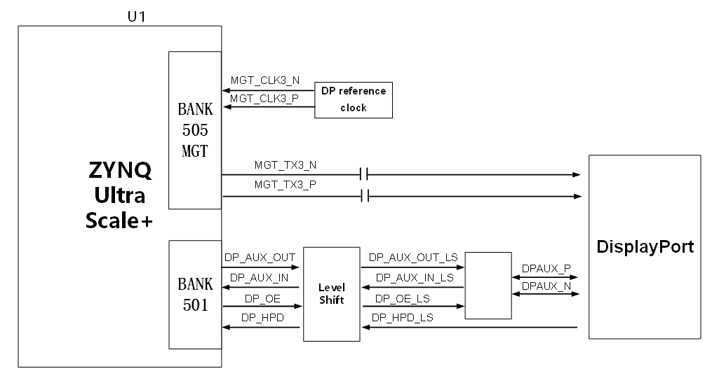
Figure 3.6.1- DP Connection Schematic
DisplayPort and ZYNQ Pin Assignment:
| Signal Name | Pin Name | Pin Number | Description |
| GT0_DP_TX_P | PS_MGT_TX3_P | AE37 | DP Data Transmit Positive |
| GT0_DP_TX_N | PS_MGT_TX3_N | AE38 | DP Data Transmit Negative |
| PS_MGT_DP_CLK_P | PS_MGT_CLK3_P | AB34 | DP Reference Clock Positive |
| PS_MGT_DP_CLK_N | PS_MGT_CLK3_N | AB35 | DP Reference Clock Negative |
| DP_AUX_OUT | BANK501_PS_MIO27 | B34 | DP Auxiliary Data Output |
| DP_AUX_IN | BANK501_PS_MIO30 | C34 | DP Auxiliary Data Input |
| DP_OE | BANK501_PS_MIO29 | B33 | DP Auxiliary Data Output Enable |
| DP_HPD | BANK501_PS_MIO28 | A33 | DP Insertion Signal Detection |
Table3.6.1- DP Pin Assignment
3.7 Optical Fiber Interface
The AXRF49 carrier board is equipped with two QSFP28 optical fiber interfaces, each connected to the GTY transceivers on BANK130 and BANK131 of the ZYNQ device.
For BANK130, the reference clocks are supplied by the LMK04828 (configurable) on the ACRF49 SoM and by a 156.25 MHz differential oscillator on the carrier board. The reference clock for BANK131 is provided by a 156.25 MHz differential oscillator located on the carrier board.
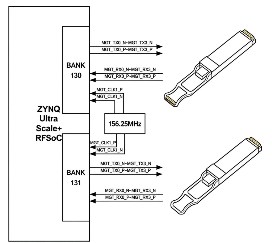
Figure3.7.1- Optical Fiber Design Schematic
J12 QSFP Interface Pin Assignment:
| Signal Name | Pin Name | Pin Number |
| QSFP_RX0_N | MGTYRXN0_130 | L42 |
| QSFP_RX0_P | MGTYRXP0_130 | L41 |
| QSFP_RX1_N | MGTYRXN1_130 | J42 |
| QSFP_RX1_P | MGTYRXP1_130 | J41 |
| QSFP_RX2_N | MGTYRXN2_130 | G42 |
| QSFP_RX2_P | MGTYRXP2_130 | G41 |
| QSFP_RX3_N | MGTYRXN3_130 | F40 |
| QSFP_RX3_P | MGTYRXP3_130 | F39 |
| QSFP_TX0_N | MGTYTXN0_130 | K39 |
| QSFP_TX0_P | MGTYTXP0_130 | K38 |
| QSFP_TX1_N | MGTYTXN1_130 | J37 |
| QSFP_TX1_P | MGTYTXP1_130 | J36 |
| QSFP_TX2_N | MGTYTXN2_130 | H39 |
| QSFP_TX2_P | MGTYTXP2_130 | H38 |
| QSFP_TX3_N | MGTYTXN3_130 | G37 |
| QSFP_TX3_P | MGTYTXP3_130 | G36 |
Table3.7.1- J12 QSFP Interface Pin Assignment
J14 QSFP Interface Pin Assignment:
| Signal Name | Pin Name | Pin Number |
| QSFP_RX0_N | MGTYRXN0_131 | E42 |
| QSFP_RX0_P | MGTYRXP0_131 | E41 |
| QSFP_RX1_N | MGTYRXN1_131 | D40 |
| QSFP_RX1_P | MGTYRXP1_131 | D39 |
| QSFP_RX2_N | MGTYRXN2_131 | C42 |
| QSFP_RX2_P | MGTYRXP2_131 | C41 |
| QSFP_RX3_N | MGTYRXN3_131 | B40 |
| QSFP_RX3_P | MGTYRXP3_131 | B39 |
| QSFP_TX0_N | MGTYTXN0_131 | F35 |
| QSFP_TX0_P | MGTYTXP0_131 | F34 |
| QSFP_TX1_N | MGTYTXN1_131 | E37 |
| QSFP_TX1_P | MGTYTXP1_131 | E36 |
| QSFP_TX2_N | MGTYTXN2_131 | C37 |
| QSFP_TX2_P | MGTYTXP2_131 | C36 |
| QSFP_TX3_N | MGTYTXN3_131 | A37 |
| QSFP_TX3_P | MGTYTXP3_131 | A36 |
Table3.7.2- J14 QSFP Interface Pin Assignment
Reference Clock Assignment:
| Pin Name | Pin Number | Description |
| MGTREFCLK0N_130 | P35 | SDCLKOUT5 output from LMK04828 |
| MGTREFCLK0P_130 | P34 | SDCLKOUT5 output from LMK04828 |
| MGTREFCLK1N_130 | M35 | Carrier board 156.25MHz crystal differential output |
| MGTREFCLK1P_130 | M34 | Carrier board 156.25MHz crystal differential output |
| MGTREFCLK1N_131 | H35 | Carrier board 156.25MHz crystal differential output |
| MGTREFCLK1P_131 | H34 | Carrier board 156.25MHz crystal differential output |
Table3.7.3- Reference Clock Assignment
J12 Optical Fiber Low-Speed IO Signal Handling Method:
| QSFP Low-Speed IO Signal Name | Remarks | SFP Low-Speed IO Signal Name | Remarks | |
| SCL | Pull-up 3.3V | TX_FULT | Pull-up 3.3V | |
| SDA | Pull-up 3.3V | TX_DISABLE | Ground | |
| ModSeIL | Pull-up 3.3V | RATE_SELECT0 | Pull-up 3.3V | |
| ResetL | Pull-up 3.3V | RATE_SELECT1 | Pull-up 3.3V | |
| ModPrsl | Pull-up 3.3V | LOS | Pull-up 3.3V | |
| intL | Pull-up 3.3V | |||
| LPMode | Ground | |||
Table3.7.4- J12 Optical Fiber Low-Speed IO Signal
J14 Optical Fiber Low-Speed IO Signal Handling Method
| QSFP Low-Speed IO Signal Name | Remarks | SFP Low-Speed IO Signal Name | Remarks | |
| SCL | Pull-up 3.3V | TX_FULT | Pull-up 3.3V | |
| SDA | Pull-up 3.3V | TX_DISABLE | Ground | |
| ModSeIL | Pull-up 3.3V | RATE_SELECT0 | Pull-up 3.3V | |
| ResetL | Pull-up 3.3V | RATE_SELECT1 | Pull-up 3.3V | |
| ModPrsl | Pull-up 3.3V | LOS | Pull-up 3.3V | |
| intL | Pull-up 3.3V | |||
| LPMode | Ground | |||
Table3.7.5- J14 Optical Fiber Low-Speed IO Signal
3.8 JTAG & UART Interface
The AXRF49 carrier board provides a JTAG & UART interface for downloading and debugging FPGA programs, as well as for programming the onboard FLASH. It uses the FTDI FT2232H, a fifth-generation high-speed USB 2.0 to UART/FIFO device. The FT2232H integrates two multi-protocol synchronous serial engines (MPSSE), enabling JTAG functionality and supporting a wide range of industry-standard serial and parallel interface configurations.The schematic diagram of the JTAG & UART connection is shown below:
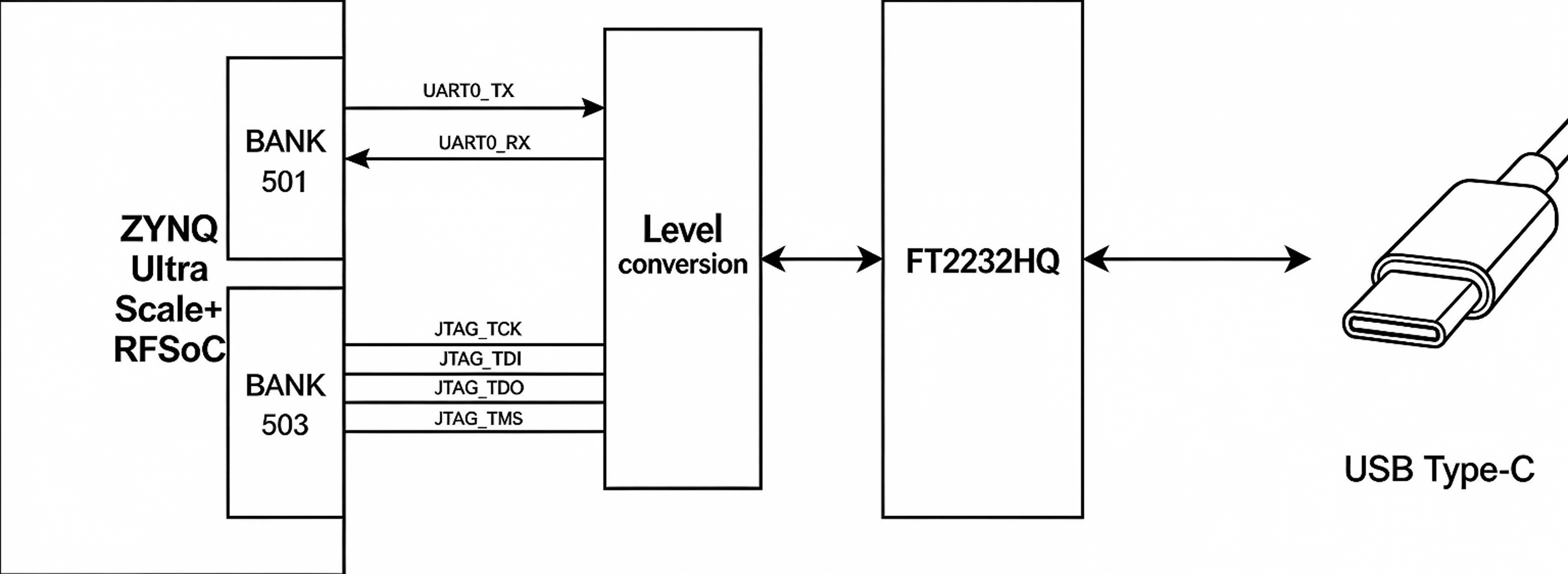
Figure 3.8.1- Schematic of JTAG & UART Connector Connection
JTAG & UART Connector pin assignment:
| Signal Name | Pin Name | Pin Number | Remarks |
| UART0_TX | BANK501_PS_MIO39 | J32 | PS Uart Data Output |
| UART0_RX | BANK501_PS_MIO38 | G32 | PS Uart Data Input |
Table3.8.1- JTAG & UART Connector Pin Assignment
3.9 GPS Module
The AXRF49 carrier board can be equipped with a NEO-M8N GPS module, a high-performance GNSS receiver known for its excellent positioning accuracy and sensitivity. This module is built on the latest u-blox M8 chipset and supports multiple satellite constellations, including GPS, GLONASS, BeiDou, and Galileo, providing reliable global positioning data.
The connection schematic for the GPS interface is shown below.
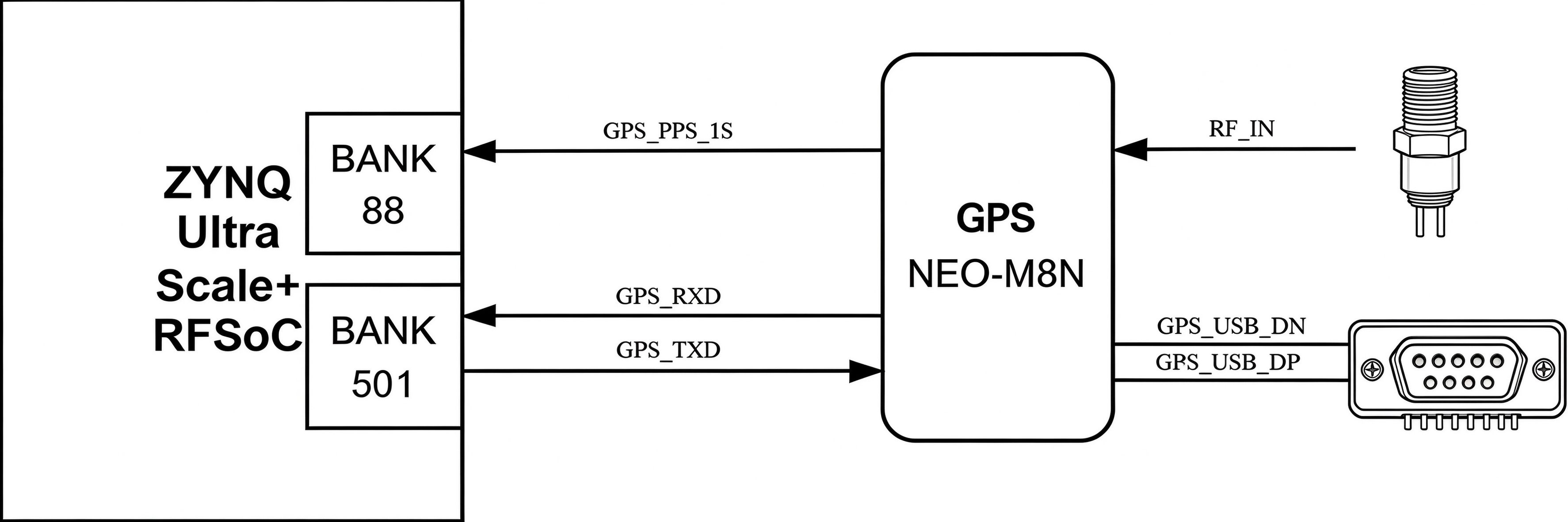
Figure3.9.1- Schematic of GPS Module Connection
GPS Module Pin Assignment:
| Signal Name | Pin Name | Pin Number | Remarks |
| PPS_1S_GPS | IO_L4N_AD12N_88 | L17 | TIMEPLUSE |
| TXD_GPS | BANK501_PS_MIO40 | F32 | TXD_MISO |
| RXD_GPS | BANK501_PS_MIO41 | K32 | RXD_MOSI |
Table3.9.1- GPS Module Pin Assignment
3.10 FMC+ Interface
The AXRF49 provides one FMC+ expansion port, enabling external connection to Xilinx or third-party FMC/FMC+ modules. This FMC+ interface includes 69 pairs of differential I/O signals and 8 GTY transceiver lanes.
The 69 differential I/O pairs are routed to the Zynq device’s BANK64, BANK65, and BANK66 I/O banks, operating at 1.8V and supporting LVDS differential signaling. The 8 GTY transceiver lanes are connected to BANK128 and BANK129.
3.11 Board-to-Board High-Speed Connector
The AXRF49 includes two surface-mounted board-to-board rectangular connectors, each with 80 pins and a 0.8 mm pitch, compatible with a 5 mm stacking height.
J3 Connector Pin Assignment:
| Signal Name | J3 Sequence | ZYNQ Pin Name | Pin Number |
| HD_IO_C_P4 | 3 | IO_L2P_AD10P_89 | J12 |
| HD_IO_C_N4 | 5 | IO_L2N_AD10N_89 | J11 |
| HD_IO_C_P5 | 9 | IO_L11P_AD1P_89 | C10 |
| HD_IO_C_N5 | 11 | IO_L11N_AD1N_89 | B10 |
| HD_IO_C_P6 | 15 | IO_L12P_AD0P_89 | A10 |
| HD_IO_C_N6 | 17 | IO_L12N_AD0N_89 | A9 |
| HD_IO_C_P7 | 21 | IO_L7P_HDGC_AD5P_89 | E10 |
| HD_IO_C_N7 | 23 | IO_L7N_HDGC_AD5N_89 | E9 |
| HD_IO_C_P8 | 27 | IO_L12P_AD0P_89 | H11 |
| HD_IO_C_N8 | 29 | IO_L12N_AD0N_89 | G10 |
| HD_IO_C_P9 | 33 | IO_L3P_AD9P_89 | H10 |
| HD_IO_C_N9 | 35 | IO_L3N_AD9N_89 | H9 |
| HD_IO_C_P10 | 39 | IO_L9P_AD3P_89 | D9 |
| HD_IO_C_N10 | 41 | IO_L9N_AD3N_89 | C9 |
| HD_IO_C_P11 | 45 | IO_L5P_HDGC_AD7P_89 | G12 |
| HD_IO_C_N11 | 47 | IO_L5N_HDGC_AD7N_89 | G11 |
Table3.11.1- J3 Connector Pin Assignment
J6 Connector Pin Assignment:
| Signal Name | J6 Sequence | ZYNQ Pin Name | Pin Number |
| HD_IO_B_P0 | 3 | IO_L6P_HDGC_87 | F15 |
| HD_IO_B_N0 | 5 | IO_L6N_HDGC_87 | E14 |
| HD_IO_B_P1 | 9 | IO_L7P_HDGC_87 | C15 |
| HD_IO_B_N1 | 11 | IO_L7N_HDGC_87 | C14 |
| HD_IO_B_P2 | 15 | IO_L8P_HDGC_87 | B16 |
| HD_IO_B_N2 | 17 | IO_L8N_HDGC_87 | B15 |
| HD_IO_B_P3 | 21 | IO_L11P_AD9P_87 | A15 |
| HD_IO_B_N3 | 23 | IO_L11N_AD9N_87 | A14 |
| HD_IO_B_P4 | 27 | IO_L10P_AD10P_87 | D16 |
| HD_IO_B_N4 | 29 | IO_L10N_AD10N_87 | C16 |
| HD_IO_B_P5 | 33 | IO_L3P_AD13P_87 | D14 |
| HD_IO_B_N5 | 35 | IO_L3N_AD13N_87 | C13 |
| HD_IO_B_P6 | 39 | IO_L5P_HDGC_87 | A13 |
| HD_IO_B_N6 | 41 | IO_L5N_HDGC_87 | A12 |
| HD_IO_B_P7 | 45 | IO_L9P_AD11P_87 | E16 |
| HD_IO_B_N7 | 47 | IO_L9N_AD11N_87 | E15 |
| HD_IO_B_P8 | 4 | IO_L1P_AD15P_87 | F12 |
| HD_IO_B_N8 | 6 | IO_L1N_AD15N_87 | E12 |
| HD_IO_B_P9 | 10 | IO_L12P_AD8P_87 | F14 |
| HD_IO_B_N9 | 12 | IO_L12N_AD8N_87 | F13 |
| HD_IO_B_P10 | 16 | IO_L2P_AD14P_87 | D13 |
| HD_IO_B_N10 | 18 | IO_L2N_AD14N_87 | D12 |
| HD_IO_B_P11 | 22 | IO_L4P_AD12P_87 | B13 |
| HD_IO_B_N11 | 24 | IO_L4N_AD12N_87 | B12 |
| HD_IO_C_P0 | 28 | IO_L8P_HDGC_AD4P_89 | E11 |
| HD_IO_C_N0 | 30 | IO_L8N_HDGC_AD4N_89 | D11 |
| HD_IO_C_P1 | 34 | IO_L6P_HDGC_AD6P_89 | F10 |
| HD_IO_C_N1 | 36 | IO_L6N_HDGC_AD6N_89 | F9 |
| HD_IO_C_P2 | 40 | IO_L10P_AD2P_89 | C11 |
| HD_IO_C_N2 | 42 | IO_L10N_AD2N_89 | B11 |
| HD_IO_C_P3 | 46 | IO_L1P_AD11P_89 | K12 |
| HD_IO_C_N3 | 48 | IO_L1N_AD11N_89 | K11 |
Table3.11.2- J6 Connector Pin Assignment
3.12 Extended IO and LED Indicators
The AXRF49 carrier board provides two groups of PL-side IOs (x7, x8) and one group of PS-side IO (x8).
J9 Extended IO Pin Assignment:
| Signal Name | Pin Name | Pin Number |
| HD_IO_A_P2 | IO_L9P_AD11P_88 | J14 |
| HD_IO_A_N2 | IO_L9N_AD11N_88 | J13 |
| HD_IO_A_P3 | IO_L6P_HDGC_88 | K15 |
| HD_IO_A_N3 | IO_L6N_HDGC_88 | K14 |
| HD_IO_A_P4 | IO_L10P_AD10P_88 | H13 |
| HD_IO_A_N4 | IO_L10N_AD10N_88 | G13 |
| HD_IO_A_P5 | IO_L7P_HDGC_88 | K17 |
Table3.12.1- J9 Extended IO Pin Assignment
J10 Extended IO Pin Assignment:
| Signal Name | Pin Name | Pin Number |
| HD_IO_A_P6 | IO_L5P_HDGC_88 | L15 |
| HD_IO_A_N6 | IO_L5N_HDGC_88 | L14 |
| HD_IO_A_P7 | IO_L3P_AD13P_88 | N14 |
| HD_IO_A_N7 | IO_L3N_AD13N_88 | M14 |
| HD_IO_A_P8 | IO_L2P_AD14P_88 | N15 |
| HD_IO_A_N8 | IO_L2N_AD14N_88 | M15 |
| HD_IO_A_P9 | IO_L1P_AD15P_88 | N16 |
| HD_IO_A_N9 | IO_L1N_AD15N_88 | M16 |
Table3.12.2- J10 Extended IO Pin Assignment
J11 Extended IO Pin Assignment:
| Signal Name | Pin Name | Pin Number |
| BANK501_PS_MIO36 | PS_MIO36 | E31 |
| BANK501_PS_MIO37 | PS_MIO37 | E32 |
| BANK501_PS_MIO33 | PS_MIO33 | D32 |
| BANK501_PS_MIO44 | PS_MIO44 | K30 |
| BANK501_PS_MIO31 | PS_MIO31 | D33 |
| BANK501_PS_MIO32 | PS_MIO32 | D34 |
| BANK501_PS_MIO42 | PS_MIO42 | H31 |
| BANK501_PS_MIO43 | PS_MIO43 | G31 |
Table3.12.3- J11 Extended IO Pin Assignment
The AXRF49 carrier board can extend 4 user-defined LED indicators, and 4 extended IOs are connected to 2-pin TJC3 through-hole sockets.
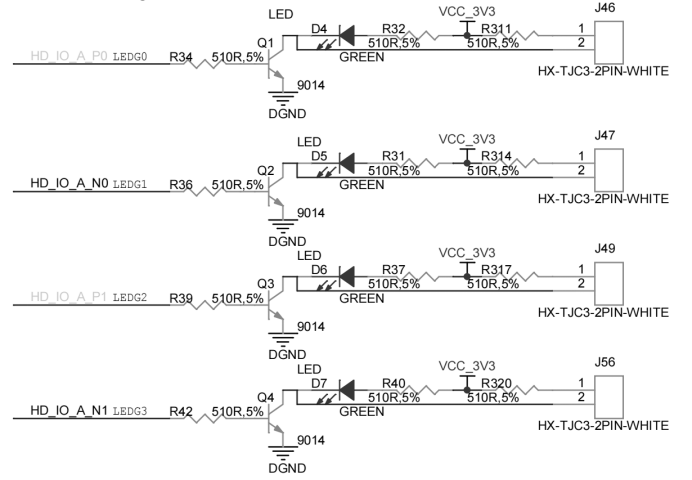
Figure3.12.2- Schematic of LED Indicator Extended IO Circuit
LED Indicator Extended IO Pin Assignment:
| Signal Name | Pin Name | Pin Number |
| LEDG0 | IO_L12P_AD8P_88 | G16 |
| LEDG1 | IO_L12N_AD8N_88 | G15 |
| LEDG2 | IO_L8P_HDGC_88 | J16 |
| LEDG3 | IO_L8N_HDGC_88 | H16 |
Table3.12.4- LED Indicator Extended IO Pin Assignment
3.13 Boot Mode Configuration
The AXRF49 carrier board includes two 2-position DIP switches, SWC1 and SWC2, which are used to configure the ZYNQ system boot mode. The AXRF49 development platform supports four boot modes: JTAG debug, QSPI Flash, eMMC, and SD card boot. After power-up, the RFSoC chip reads the logic levels of PS_MODE [0–3] to determine the boot mode. Users can select the desired boot mode using the SWC1 DIP switch.
The boot mode configuration for SWC1 and SWC2 is as follows in the table below.
| DIP Switch SWC1 Position (1, 2) | DIP Switch SWC2 Position (1, 2) | MODE [3:0] | Boot Mode |
| ON, ON | ON, ON | 0000 | JTAG |
| ON, ON | OFF, ON | 0010 | QSPI |
| ON, OFF | OFF, ON | 0110 | EMMC |
| OFF, OFF | OFF, ON | 1110 | SD |
Table 3.13.1- Boot Mode Configuration
3.14 RF Radio Frequency Link
The AXRF49 supports 16 channels of 14-bit ADC input at 2.5 GSPS and 16 channels of 14-bit DAC output at 9.85 GSPS, with single-ended analog input and output. Conversion between single-ended and differential signaling is implemented using balun components, enabling high-performance data reception and transmission.
On the ADC side, the analog front end first passes through a limiting diode, after which a balun converts the single-ended signal into a differential signal. The resulting differential signal is routed directly to the core module’s RF-ADC pins. The schematic diagram is shown below.
For the DAC path, the differential output signals from the core module’s RF-DAC are converted to single-ended signals through a balun. The single-ended signal then passes through a DC coupling module before being routed to the MCX RF connector, as shown in the schematic below.
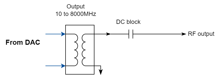
Figure3.14.2- DAC
3.15 MMCX Interface
The AXRF49 development board supports external reference clock input/output as well as trigger signal input/output.
MMCX Interface Pin Assignment:
| Signal Name | Pin Name | Pin Number | Remarks |
| CLKIN2 | J27 | LMK04828 Reference Clock Input | |
| CLKOUT | J24 | LMK04828 Clock Output | |
| TRIG_IN | JA33 | H15 | Trigger Signal Input |
| TRIG_OUT | JA34 | H14 | Trigger Signal Output |
| ADC_CLK | J25 | ADC_CLK_225 | |
| DAC_CLK | J26 | DAC_CLK_229 | |
| CLK_IN0 | J23 | LMK04828 Reference Clock Input | |
| SYSREF_IN_P | J21 | LMK04828 Reference Clock Input | |
| SYSREF_IN_N | J22 | LMK04828 Reference Clock Input |
Table 3.15.1- MMCX Interface Pin Assignment
3.16 FAN Heatsink
The AXRF49 generates significant heat during normal operation. We have added a heat dissipation structure and a fan to the core board to prevent chip overheating. The fan speed is controlled by the PL side of the ZYNQ chip, with control pins connected to the IOs on BANK88.
| Signal Name | Pin Name | Pin Number | Remarks |
| HD_IO_A_N5 | IO_L7N_HDGC_88 | K16 |
Table 3.16.1- Fan
3.17 Power Supply
The AXRF49 carrier board is powered by a 12 V DC input. The carrier board generates +5 V, +3.3 V, and +1.8 V supply rails through multiple onboard power management ICs.
The power supply block diagram is shown below:
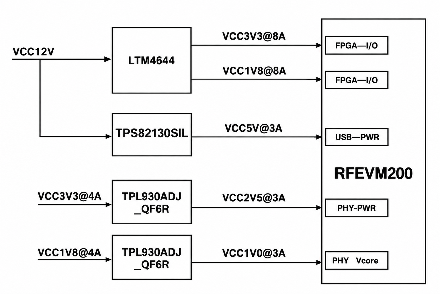
Figure 3.17.1- Carrier Board Power Supply Diagram
3.18 Mechanical Dimensions Diagram
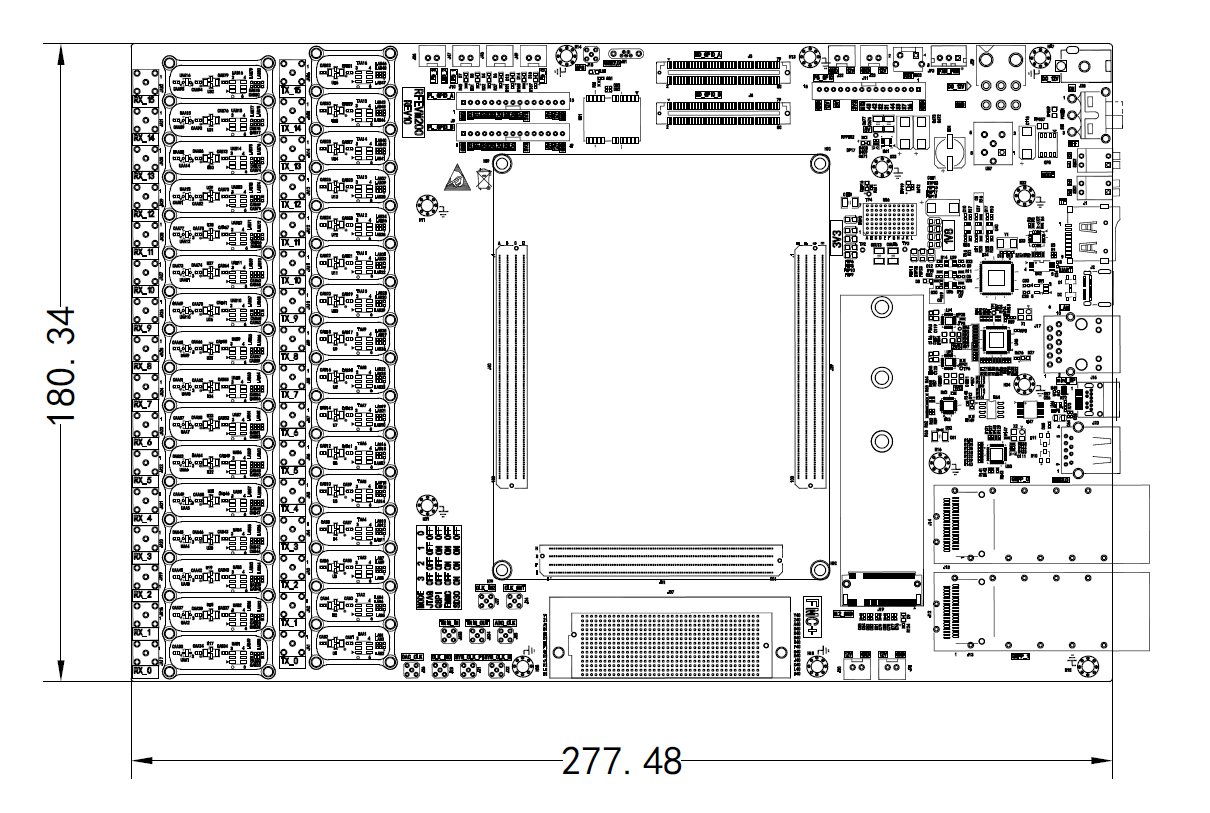
Figure 3.18.1- AXRF49 Front View
Appendix: List of Abbreviations
| Abbreviation | Full English Name | Description |
| PS | Processor System | Processor System |
| PL | Programmable Logic | Programmable Logic |
| SOC | System on Chip | System on Chip |
| DDR3 | Double Data Rate 3 SDRAM | Double Data Rate 3 SDRAM |
| eMMC | Embedded Multi Media Card | Embedded MultiMediaCard |
| QSPI | Quad Serial Peripheral Interface | Quad Serial Peripheral Interface |
| GTP | Gigabit Transceiver | Gigabit Transceiver |
| UART | Universal Asynchronous Receiver/Transmitter | Universal Asynchronous Receiver/Transmitter |
| HDMI | High-Definition Multimedia Interface | High-Definition Multimedia Interface |
| PCIe | Peripheral Component Interconnect Express | Peripheral Component Interconnect Express |
| USB | Universal Serial Bus | Universal Serial Bus |
| JTAG | Joint Test Action Group | Joint Test Action Group |
| SFP | Small Form-factor Pluggable | Small Form-factor Pluggable |
| MIO | Multiplexed I/O | Multiplexed I/O |
| GPHY | Gigabit Ethernet PHY | Gigabit Ethernet PHY |
| I2C | Inter-Integrated Circuit | Inter-Integrated Circuit |
| RGMII | Reduced Gigabit Media Independent Interface | Reduced Gigabit Media Independent Interface |
| RMII | Reduced Media Independent Interface | Reduced Media Independent Interface |
| LED | Light Emitting Diode | Light Emitting Diode |
| LVDS | Low-Voltage Differential Signaling | Low-Voltage Differential Signaling |
Contact information
Alinx Electronic Limited
Company Website: www.en.alinx.com
Service Hotline: +86 21 67676997
Technical Support:technical@alinx.com