
Appearance
AXW22 User Manual

Alinx Electronic Limited
Company Website: www.en.alinx.com
Service Hotline: +86 21 67676997
Technical Support : technical@alinx.com
Document Information
| Item | Content |
| Document Name | Product Manual |
| Product Model | AXW22 |
| Document Version | V1.0 |
| Prepared by | Alinx Electronic Limited |
| Release Date | 2026.9.30 |
Document Revision History
| Version | Date | Section | Revision Summary |
| V1.0 | 2026.9.30 | All | Initial Release |
Part 1: Overview
1.1 Product Description
The AXW22 mixed-signal processing card, based on the Xilinx ZYNQ UltraScale+ RFSoC ZU47DR, offers access to large FPGA gate density, two ADC/DAC ports, expandable I/O ports, and DDR4 memory, making it suitable for a variety of programmable applications. The AXW22 with the ZU47DR FPGA is powered by two 14-bit, 5.0 GSPS ADC ports and two 14-bit, 10 GSPS DAC ports.
The RF transmit and receive ports connect externally via high-performance SMA side-mounted RF connectors. The core processing system is based on the ZYNQ UltraScale+ RFSOC, featuring rich peripheral interfaces for transmitting control signals to the signal processing circuit. The AXW22 board includes a 40Gbps QSFP connector for optical ports and a 10Gbps SFP connector for efficient high-speed data processing in parallel with analog-to-digital conversion. The PS and PL models are equipped with 4GB DDR4 and 2GB DDR4 memory, respectively; they support MicroSD cards (UHS-compliant), 10/100/1000 Ethernet, and USB JTAG/UART interfaces. The board supports JTAG loading mode, which shares the UART output, provides one RS232 interface, integrates a GPS module, and features a GPIO expansion interface for additional functionality.
1.2 Product Features
- AXW22
The Zynq UltraScale+ RFSoC , a new innovation from Xilinx , provides such a solution. This family of devices features an integrated ADC (up to two 14 -bit channels at a sampling rate of 5.0 GSPS), a DAC (up to two 14 -bit channels at a sampling frequency of 10 GSPS), configurable logic elements, a multiprocessor embedded ARM Cortex-A53 application processing unit (APU), and an ARM real-time processing unit (RPU). Integrating all these devices offloads many analog signal processing actions (typically occurring near the antenna in a digital receiver) to the digital domain.
This helps reduce the complexity of the RF signal processing chain, standardize a flexible set of hardware to meet a variety of application needs, maximize input/output channel density without sacrificing wide bandwidth and take advantage of heterogeneous processing capabilities , all of which fully leverages the built-in security features of the Zynq architecture to help protect IP security.
The AXW22 is the third algorithm evaluation board to utilize RFSoC devices. It provides a COTS solution that offers the advantages of RFSoC while allowing for more efficient data offloading and the benefits of COTS: users can deploy as quickly as possible while taking advantage of lower ownership costs, lifecycle support, and simplified future technology insertion.
- RFSOC vs. MPSOC vs. FPGA
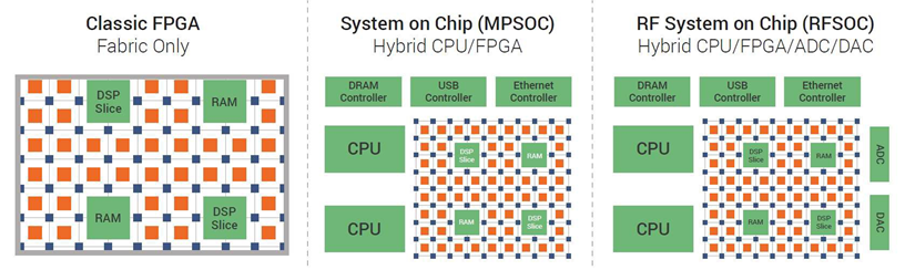
- Reduce RF signal chain complexity
Radar and EW systems with multiple channels face challenges in terms of cost and complexity, as more channels mean more expensive and extensive RF signal up/down conversion and conditioning. A common solution is direct RF sampling , a more flexible approach than traditional analog frequency conversion and filtering. Direct RF sampling can be implemented in the digital domain, consuming less power and typically at a lower cost.
This means that the RF front end can handle a wider bandwidth than traditional analog technologies while consuming less power. Similar to RFSoC devices, using a very high sampling rate in the data converter means that most of the analog filtering and conditioning can be done closer to the antenna, resulting in a simpler and more flexible front end than in the past.
Furthermore, because ADCs and DACs have historically been separate from programmable FPGAs, high-speed interfaces are required for communication between devices. The JESD204B has been a common high-speed serial interface in recent years , but it comes at the cost of latency and design complexity. For some radar or EW applications, the latency of the JESD204B is too high, and devices using this interface are often used for system integration. RFSoC helps solve this problem. By integrating the ADC and DAC into the device, the need for the JESD204B is eliminated , simplifying design complexity and helping to reduce latency.
- Maximize input/ output channel density
To counter emerging threats to electromagnetic spectrum dominance, modern radar and electronic warfare systems require increasingly more channels and wider bandwidths. The AXW22, featuring a 2- channel ADC and a 2- channel DAC, is one of the first RFSOC FPGA carrier boards launched in China, capable of synchronizing all two channels. The system incorporates multiple boards and channels to meet the demands of larger system applications. In previous generations of technology, this combination required four times the number of boards.
- Heterogeneous processing capability
Furthermore, many other systems, such as radar and electronic warfare systems, require streaming DSPs with FPGAs and general-purpose processors for decision-making and control. Previously, these processing requirements were handled by separate modules; now, with the AXW22 , both functionalities can be integrated into a single module using RFSoC technology.
This is particularly relevant to the growing demand for cognitive or intelligent radar/electronic warfare technologies. Furthermore, the simplified integration with RF sampling devices eliminates the complexity of the JESD204B high-speed serial interface. This means that basic functions such as device-to-device communication consume fewer programmable logic elements, resulting in more computational resources available for application-specific IP than in the past.
- Unload data more effectively
In addition to all the aforementioned advantages of RFSoC devices, the AXW22 also features an optional single-channel VITA66.4 fiber optic interface, which helps in more efficiently offloading data. When a system involves multiple channels and extremely high sampling rates, the challenge of how to process the data always arises; the system must perform sampling, processing, or transmission of the data within the FPGA. In many cases, the system is limited to standard data connection architectures. Two ADC channels sample at rates above 4 GSPS with each sample occupying two bytes. Even the high-speed PCIe Gen 3 data link is too slow for direct data transfer. To overcome this challenge, the AXW22 uses one 40G QSFP VITA 66.4 fiber optical interface and one 10G SFP fiber optical interface for efficient data offloading.
1.3 Instructions before use
Electrostatic discharge (ESD) may damage the components on this board. To prevent damage, please follow ESD precautions:
Always wear an anti-static wrist strap when operating this board .
When you need to manually handle a circuit board, try to place your hand on the edge of the board.
Avoid touching any components.
Store in an ESD-safe bag when not in use.
1.4 Hardware Block Diagram
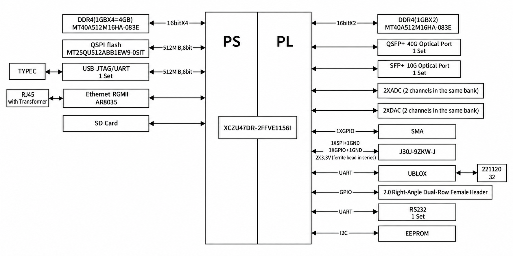
Figure 1.4.1 - Overall block diagram of the AXW22 board
Part 2: Platform Hardware Introduction
2.1 Main Specifications
| project | Specifications |
| FPGA chip | Zynq UltraScale+ XCZU47DR-2FFVE1156I RFSOC |
| RF interface | x2ADC (14-bit, 5GSPS) ports |
| x2DAC (14-bit, 10GSPS) ports | |
| 40G optical port | Route 1 |
| Memory | PS 4×DDR4 (4GB, 64bit, 2666MT/s) |
| PL 2×DDR4 (2GB, 32bit, 2666MT/s) | |
| Power supply for the board | Commonly used 2.5mm round head power socket (DC +12V) |
| PS end | • 2× QSPI Flash (512MB, 8bit) firmware configuration files |
| • 1 x 10/100/1000 Ethernet + RGMII (RJ45) port | |
| • 1 x USB JTAG UART debugging interface | |
| • 1× JTAG debugging interface | |
| • 1× Micro SD Card | |
| PL end | • 2-channel ADC (14-bit, 5GSPS) ports |
| • 2-channel DAC (14-bit, 10GSPS) ports | |
| • 1× QSFP+ 40G optical port | |
| • 1× SFP+ 10G optical port | |
| • 1-channel I2C interface EEPROM | |
| • GPS interface (interface type: side-mounted SMA connector) | |
| • 1 SPI interface and 1 GPIO interface (interface type: J30 connector) | |
| • 36× GPIOs (Interface type: 2.0mm pitch right-angle socket) | |
| • 1× RS232 interface (interface type: 2.0mm pitch right-angle socket) | |
| • 8× LEDs | |
| size | 180mm × 135mm |
| Operating temperature | -40℃ ~ 70 ℃ |
| Reference Project | • Configure ADC/DAC related registers in the host computer software |
| • High-speed ADC/DAC loopback test engineering | |
| • Schematics (PDF format) | |
| • DDR4 Reference Design | |
| • FPGA pin arrangement |
2.2 Physical Photos and Resources
The physical layout of AXW22 is shown in the figure below. This figure indicates the main components on the board, along with the types of components and their corresponding chip names; details are provided in the table below.
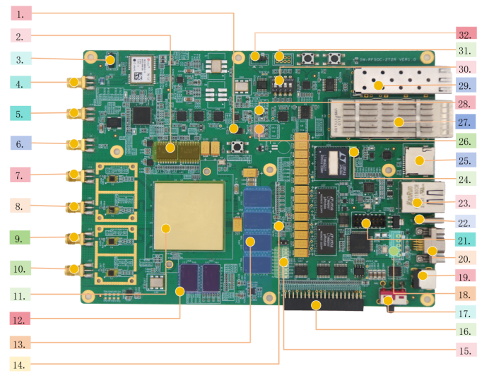
Figure 2.2.1 - Photo of the actual AXW22 board.
Note: An oval shape indicates that the component is on the front of the board
| SR.No | Designator | Description |
| 1 | U15 | PL EEPROM |
| 2 | U13, U14 | PS QSPI Flash |
| 3 | J7 | Reserved USB port for interacting with GPS information with other devices through the USB interface |
| 4 | J6 | GPS Input signal |
| 5 | J16 | Input clock signal of the clock generator |
| 6 | J1 | Clock Input |
| 7 | J11 | DAC1 Output (SMA) |
| 8 | J10 | DAC0 Output (SMA) |
| 9 | J13 | ADC1 Input (SMA) |
| 10 | J12 | ADC0 Input (SMA) |
| 11 | U1 | RFSOC Main Chip (XCZU47DR) |
| 12 | U54,U55 | PL DDR4 |
| 13 | U50,U51,U52,U53 | PS DDR4 |
| 14 | J18 | Reserved Fan Interface(5V) |
| 15 | DS7 | PL LED7 |
| DS8 | PL LED6 | |
| DS9 | PL LED5 | |
| DS10 | PL LED4 | |
| DS11 | PL LED3 | |
| DS12 | PL LED2 | |
| DS13 | PL LED1 | |
| DS14 | PL LED0 | |
| 16 | J8 | PL 36 GPIO Reserved Interface |
| 17 | SW2 | Power Switch |
| 18 | U20 | USB-JTAG Debugging Interface, used to route to the chassis |
| 19 | J14 | Main Power Supply (DC 12V) |
| 20 | J9 | 1 PL GPIO reserved interface, 1 SPI interface |
| 21 | J4 | JTAG Debug Interface |
| 22 | J3 | USB Type-C (USB-JTAG/UART) |
| 23 | J5 | PS Gigabit Ethernet Port |
| 24 | J17 | Reserved Fan Interface(12V) |
| 25 | CN1 | PS Micro SD Card Slot |
| 26 | DS2 | PS_DONE Status Light |
| DS1 | PS_INIT_B Status Light | |
| 27 | DS4 | PS_ERR_STATUS Indicator Light |
| DS3 | PS_ERR_OUT Indicator Light | |
| 28 | U2 | 40G QSFP+ Optical Port |
| 29 | U30 | PL 10G SFP+ Optical Port |
| 30 | SW1 | Boot Mode Configuration Switch |
| 31 | J2 | Startup mode configuration switch, used for leading to the front panel |
| 32 | J15 | PL RS232 Interface |
Table 2.2.1 - Location of Main Components
Part 3: Platform Resources Details
3.1 FPGA Chip
The AXW22 is based on the Zynq UltraScale+ XCZU47DR-2FFVE1156 device, integrating the Processing System (PS) and Programmable Logic (PL) on a single chip. The PS section within the Zynq UltraScale+ RFSoC consists of a 64-bit quad-core Cortex®-A53 processor and a dual-core Cortex-R5 real-time processor. Its on-chip resources are listed below:
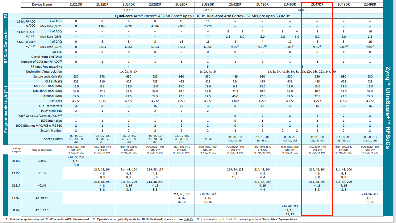
Figure 3.1.1 - XCZU47DR-2FFVE1156 chip resources
3.2 BANK Voltage
The voltages of each bank on the main chip of the AXW22 board are shown in the table below.
| XCZU47DR-BANK | POWER NET | Voltage |
| PL BANK 65 | VCC1V2 | 1.2V |
| PL BANK 66 | VCC1V2 | 1.2V |
| PL BANK 88 | UTIL_3V3 | 3.3V |
| PL BANK 89 | UTIL_3V3 | 3.3V |
| PS BANK 500 | VCC1V8 | 1.8V |
| PS BANK 501 | VCC1V8 | 1.8V |
| PS BANK 502 | VCC1V8/UTIL_3V3 | 1.8V/3.3V |
| PS BANK 503 | VCC1V8 | 1.8V |
| PS BANK 504 | VCC1V2 | 1.2V |
Table 3.2.1 - XCZU47DR-2FFVE1156 BANK Voltage
3.3 Board Boot Mode Configuration
AXW22 selects the device configuration method through SW1 , and the relevant schematic diagram is shown below.
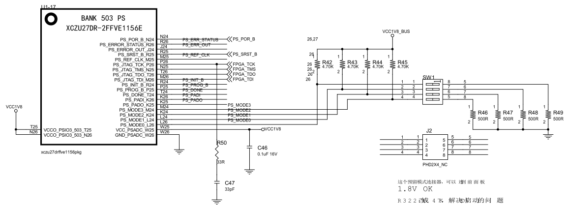
Figure 3.3.1 - AXW22 PS-MODE Configuration Principle Diagram
The configuration modes corresponding to each state of SW 1 are shown in the table below .
| BOOT mode | Mode pin configuration [3:0] | SW1 DIP switch configuration [4:1] |
| PS JTAG | 0000 | ON,ON,ON,ON |
| Quad-SPI (32b) | 0010 | ON, ON, OFF, ON |
| SD1(2.0) | 0101 | ON, OFF, ON, OFF |
Table 3.3.1 - XCZU47DR-2FFVE1156 SW1 Mode Configuration Table
PS JTAG mode, a JTAG connection can be established with the board via connector J4 or J3 (TYPE C) ;
Quad- SPI (32b) mode, QSPI memory boot can be enabled through configuration; see the QSPI Flash module for details .
SD1 (2.0) card mode, SD card boot can be enabled through configuration; see the SD module for details .
3.4 Clock
The Zynq UltraScale RFSoC offers a variety of clock options, and the board features a user-programmable clock generator. These clocks can be used in conjunction with the FPGA's internal PLL to accommodate various communication protocols. A block diagram of the RF clock section is shown below.
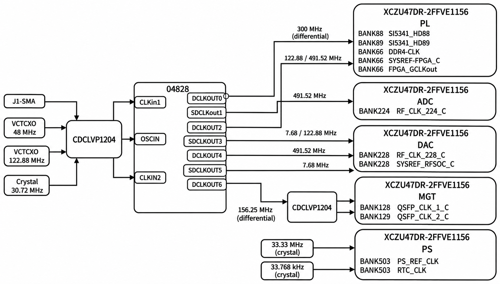
Figure 3.4.1 - Overall block diagram of the clock section
The clock generator has two clock inputs: one is the clock signal input from the SMA connector, and the other is provided by the local clock chip. The clock generator is used to provide the ADC sampling clock, DAC sampling clock, and QSFP, SFP clock, etc.
Two SYSREF clocks provide a reference clock function for synchronizing the RF ADC and DAC; these are also obtained by dividing the clock generator . The schematic diagram of the clock generator section is shown below.
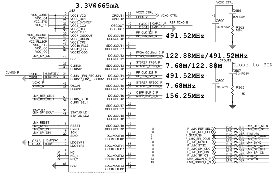
Figure 3.4.2 - Schematic diagram of the clock generator .
| Signal | Frequency | Target FPGA Input | FPGA PIN |
| RF_CLK_224_P | Variable | RF_CLK_224_C_P | AD5 |
| RF_CLK_224_N | Variable | RF_CLK_224_C_N | AD4 |
| RF_CLK_228_P | Variable | RF_CLK_228_C_P | L5 |
| RF_CLK_228_N | Variable | RF_CLK_228_C_N | L4 |
| FPGA_GCLKout_C_P | Variable | FPGA_GCLKout_P | AP11 |
| FPGA_GCLKout_C_N | Variable | FPGA_GCLKout_N | AP10 |
| SYSREF_FPGA_P | Variable | SYSREF_FPGA_C_P | AM10 |
| SYSREF_FPGA_N | Variable | SYSREF_FPGA_C_N | AN10 |
| SYSREF_RFSOC_P | Variable | SYSREF_RFSOC_C_P | N5 |
| SYSREF_RFSOC_N | Variable | SYSREF_RFSOC_C_N | N4 |
Table 3.4.1 - Relationship between clock generator frequency division clock and RFSOC
Note: Differential clocks only need to be bound to the P terminal.
| Signal | Frequency | Target BUFFER Input | BUFFER PIN |
| QSFP_BUF_C_P | Variable | QSFP_BUF_P | 3 |
| QSFP_BUF_C_ N | Variable | QSFP_BUF_N | 4 |
Table 3.4.2 - Relationship between Clock Generator Divided Clock and QSFP Clock
The clock sources for this board are shown in the table below.
| Signal | Frequency | CLK SOURCE | FPGA PIN |
| PS_REF_CLK | 33.33MHz | 33.33MHz active crystal oscillator | M25 : PS_REF_CLK_M25 |
| PS_PADI/PADO | 32.768kHz | 32.768kHz passive crystal | K26: PS_PADI_K26 K25 : PS_PADO_K25 |
| DDR4_PL_300M_N DDR4_PL_300M_P | 300MHz | LVDS Differential Crystal Oscillator | AM9 : IO_L13N_T2L_N1_GC_QBC_66_AM9 AL9 : IO_L13P_T2L_N0_GC_QBC_66_AL9 |
| QSFP_CLK_1_C_P QSFP_CLK_1_C_N | 156.25MHz | clock buffer | M28 : MGTREFCLK0P_128_M28 M29 : MGTREFCLK0N_128_M29 |
| QSFP_CLK_2_C_P QSFP_CLK_2_C_N | 156.25MHz | clock buffer | H28 : MGTREFCLK0P_129_H28 H29 : MGTREFCLK0N_129_H29 |
Table 3.4.3 - Clock Source Relationship Table (DDR, QSFP, etc.)
3.5 PS DDR4 & PL DDR4
AXW22 provides a 4GB, 64-bit memory system consisting of four 512Mb*16 DDR4 chips (U50 , U51 , U52 , U53 ). This memory system is connected to the hard-core memory controller BANK 504 on the PS side of the main chip (see the schematic section for details).
AXW22 also provides a 2 GB, 32-bit wide memory system consisting of two 512Mb*16 DDR4 chips (U54 , U55 ), which are connected to BANK 66 and BANK 65 on the PL side of the main chip . The overall block diagram of DDR4 on the PS and PL sides is shown in the figure below.
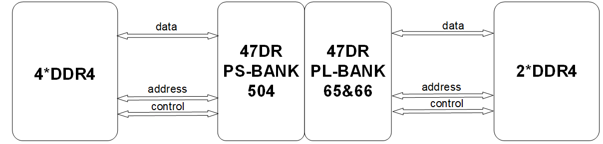
Figure 3.5.1 - Overall block diagram of DDR4
The relevant schematic diagram is shown below. U50 is used as an example here. The schematic diagrams of other DDR4 chips are the same as those of U50, and will not be listed here.
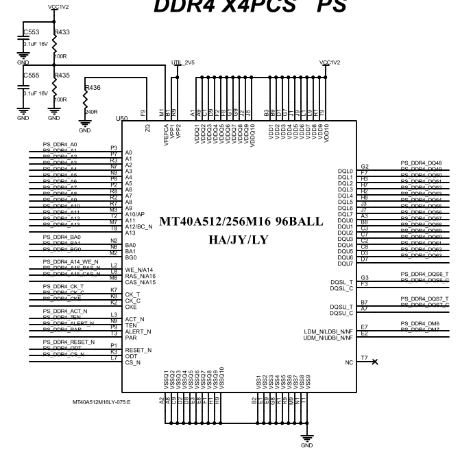
Figure 3.5.2 - Schematic diagram of DDR4 related principles
| 47DR PIN | Schematic Net Name |
| AG12: IO_L19P_T3L_N0_DBC_AD9P_66_ AG12 | PL_DDR4_A0 |
| AJ11: IO_L18P_T2U_N10_AD2P_66_AJ11 | PL_DDR4_A1 |
| AH10: IO_L20P_T3L_N2_AD1P_66_AH10 | PL_DDR4_A2 |
| AH9: IO_L20N_T3L_N3_AD1N_66_AH9 | PL_DDR4_A3 |
| AG10: IO_L21P_T3L_N4_AD8P_66_AG10 | PL_DDR4_A4 |
| AG9: IO_L21N_T3L_N5_AD8N_66_AG9 | PL_DDR4_A5 |
| AM11: IO_L14N_T2L_N3_GC_66_AM11 | PL_DDR4_A6 |
| AG11: IO_L19N_T3L_N1_DBC_AD9N_66_AG11 | PL_DDR4_A7 |
| AE11: IO_L24P_T3U_N10_66_AE11 | PL_DDR4_A8 |
| AF10: IO_L24N_T3U_N11_66_AF10 | PL_DDR4_A9 |
| AM12: IO_L14P_T2L_N2_GC_66_AM12 | PL_DDR4_A10 |
| AF12: IO_L23P_T3U_N8_66_AF12 | PL_DDR4_A11 |
| AL12: IO_L16P_T2U_N6_QBC_AD3P_66_AL12 | PL_DDR4_A12 |
| AF11: IO_L23N_T3U_N9_66_AF11 | PL_DDR4_A13 |
| AK9: IO_L17N_T2U_N9_AD10N_66_AK9 | PL_DDR4_BA0 |
| AK10: IO_L17P_T2U_N8_AD10P_66_AK10 | PL_DDR4_BA1 |
| AP12: IO_L7N_T1L_N1_QBC_AD13N_66_AP12 | PL_DDR4_BG0 |
| AN12: IO_L8N_T1L_N3_AD5N_66_AN12 | PL_DDR4_A14_WE_N |
| AL13: IO_L15N_T2L_N5_AD11N_66_AL13 | PL_DDR4_A16_RAS_N |
| AL11: IO_L16N_T2U_N7_QBC_AD3N_66_AL11 | PL_DDR4_A15_CAS_N |
| AJ10: IO_L22P_T3U_N6_DBC_AD0P_66_AJ10 | PL_DDR4_CK_T |
| AJ9: IO_L22N_T3U_N7_DBC_AD0N_66_AJ9 | PL_DDR4_CK_C |
| AN13: IO_L8P_T1L_N2_AD5P_66_AN13 | PL_DDR4_CKE |
| AN8: IO_L9P_T1L_N4_AD12P_66_AN8 | PL_DDR4_ACT_N |
| AN7:IO_L9N_T1L_N5_AD12N_66_AN7 | PL_DDR4_RESET_N |
| AK13: IO_L15P_T2L_N4_AD11P_66_AK13 | PL_DDR4_ODT |
| AP13: IO_L7P_T1L_N0_QBC_AD13P_66_AP13 | PL_DDR4_CS_N |
| AC16: IO_L22P_T3U_N6_DBC_AD0P_65_AC16 | PL_DDR4_DQS0_T |
| AC15: IO_L22N_T3U_N7_DBC_AD0N_65_AC15 | PL_DDR4_DQS0_C |
| AG14: IO_L16P_T2U_N6_QBC_AD3P_65_AG14 | PL_DDR4_DQS1_T |
| AH14: IO_L16N_T2U_N7_QBC_AD3N_65_AH14 | PL_DDR4_DQS1_C |
| AH18: IO_L10P_T1U_N6_QBC_AD4P_65_AH18 | PL_DDR4_DQS2_T |
| AJ18: IO_L10N_T1U_N7_QBC_AD4N_65_AJ18 | PL_DDR4_DQS2_C |
| AL17: IO_L4P_T0U_N6_DBC_AD7P_SMBALERT_65_AL17 | PL_DDR4_DQS3_T |
| AM16: IO_L4N_T0U_N7_DBC_AD7N_65_AM16 | PL_DDR4_DQS3_C |
| AC13: IO_L19P_T3L_N0_DBC_AD9P_65_AC13 | PL_DDR4_DM0 |
| AG15: IO_L13P_T2L_N0_GC_QBC_65_AG15 | PL_DDR4_DM1 |
| AH13: IO_L7P_T1L_N0_QBC_AD13P_65_AH13 | PL_DDR4_DM2 |
| AM14: IO_L1P_T0L_N0_DBC_65_AM14 | PL_DDR4_DM3 |
| AE14: IO_L20P_T3L_N2_AD1P_65_AE14 | PL_DDR4_DQ0 |
| AD16: IO_L23N_T3U_N9_65_AD16 | PL_DDR4_DQ1 |
| AE15: IO_L21N_T3L_N5_AD8N_65_AE15 | PL_DDR4_DQ2 |
| AC17: IO_L23P_T3U_N8_I2C_SCLK_65_AC17 | PL_DDR4_DQ3 |
| AD15: IO_L21P_T3L_N4_AD8P_65_AD15 | PL_DDR4_DQ4 |
| AE18: O_L24N_T3U_N11_PERSTN0_65_AE18 | PL_DDR4_DQ5 |
| AE13: IO_L20N_T3L_N3_AD1N_65_AE13 | PL_DDR4_DQ6 |
| AD18: IO_L24P_T3U_N10_PERSTN1_I2C_SDA_65_AD18 | PL_DDR4_DQ7 |
| AF13: IO_L15N_T2L_N5_AD11N_65_AF13 | PL_DDR4_DQ8 |
| AG17: IO_L14P_T2L_N2_GC_65_AG17 | PL_DDR4_DQ9 |
| AE16: IO_L17P_T2U_N8_AD10P_65_AE16 | PL_DDR4_DQ10 |
| AH17: IO_L14N_T2L_N3_GC_65_AH17 | PL_DDR4_DQ11 |
| AF14: IO_L15P_T2L_N4_AD11P_65_AF14 | PL_DDR4_DQ12 |
| AF17: IO_L18N_T2U_N11_AD2N_65_AF17 | PL_DDR4_DQ13 |
| AF16: IO_L17N_T2U_N9_AD10N_65_AF16 | PL_DDR4_DQ14 |
| AF18: IO_L18P_T2U_N10_AD2P_65_AF18 | PL_DDR4_DQ15 |
| AK15: IO_L8P_T1L_N2_AD5P_65_AK15 | PL_DDR4_DQ16 |
| AK18: IO_L9P_T1L_N4_AD12P_65_AK18 | PL_DDR4_DQ17 |
| AK16: IO_L12N_T1U_N11_GC_65_AK16 | PL_DDR4_DQ18 |
| AJ15: IO_L11N_T1U_N9_GC_65_AJ15 | PL_DDR4_DQ19 |
| AK14: IO_L8N_T1L_N3_AD5N_65_AK14 | PL_DDR4_DQ20 |
| AL18: IO_L9N_T1L_N5_AD12N_65_AL18 | PL_DDR4_DQ21 |
| AJ16: IO_L11P_T1U_N8_GC_65_AJ16 | PL_DDR4_DQ22 |
| AJ17: IO_L12P_T1U_N10_GC_65_AJ17 | PL_DDR4_DQ23 |
| AN17: IO_L5N_T0U_N9_AD14N_65_AN17 | PL_DDR4_DQ24 |
| AN18: IO_L6P_T0U_N10_AD6P_65_AN18 | PL_DDR4_DQ25 |
| AP16: IO_L3P_T0L_N4_AD15P_65_AP16 | PL_DDR4_DQ26 |
| AP17: IO_L6N_T0U_N11_AD6N_65_AP17 | PL_DDR4_DQ27 |
| AP15: IO_L3N_T0L_N5_AD15N_65_AP15 | PL_DDR4_DQ28 |
| AM17: IO_L5P_T0U_N8_AD14P_65_AM17 | PL_DDR4_DQ29 |
| AM15: IO_L2P_T0L_N2_65_AM15 | PL_DDR4_DQ30 |
| AN15: IO_L2N_T0L_N3_65_AN15 | PL_DDR4_DQ31 |
Table 3.5.1 - PL-side DDR4 pin assignment
3.6 PS QSPI Flash
The AXW22 evaluation board has an onboard 2Gb Flash Memory uses two Micron serial NOR flash QSPI memories to store executable code and data such as bootloaders, operating systems, and bitstreams in 47DR PS and PL.
To achieve higher performance, two Quad-SPI devices are connected in parallel, providing a total of 8 bits for booting and configuration. The device numbers are U13 and U14 , and they can only be accessed by the PS.
QSPI Flash Memory specifications for configuration and data storage:
Model: MT25QU01GBBB8ESF-0SIT (Micron)
Power supply voltage: 1.8V
Data width: 4 bits
Data rate: depends on single, dual, or quad mode
The chip pins correspond to MIO0-MIO5 and MIO7-MIO12 in BANK500.
The overall block diagram of the QSPI Flash section is shown in the figure below.
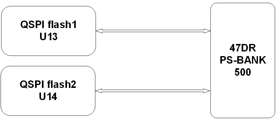
Figure 3.6.1 - PS QSPI Flash Schematic Diagram
The schematic diagram for this part is shown below.
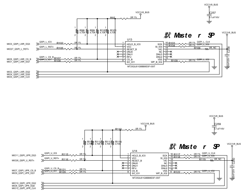
Figure 3.6.2 - Schematic diagram of PS QSPI Flash principle
| 47DR PIN | Schematic Net Name |
| J17: PS_MIO0_J17 | MIO0_QSPI_LWR_CLK |
| J18: PS_MIO1_J18 | MIO1_QSPI_LWR_DQ1 |
| J16: PS_MIO2_J16 | MIO2_QSPI_LWR_DQ2 |
| K16: PS_MIO3_K16 | MIO3_QSPI_LWR_DQ3 |
| G15: PS_MIO4_G15 | MIO4_QSPI_LWR_DQ0 |
| H18: PS_MIO5_H18 | MIO5_QSPI_LWR_CS_B |
| K17: PS_MIO7_K17 | MIO7_QSPI_UPR_CS_B |
| E15: PS_MIO8_E15 | MIO8_QSPI_UPR_DQ0 |
| F15: PS_MIO9_F15 | MIO9_QSPI_UPR_DQ1 |
| C15: PS_MIO10_C15 | MIO10_QSPI_UPR_DQ2 |
| G16: PS_MIO11_G16 | MIO11_QSPI_UPR_DQ3 |
| B15: PS_MIO12_B15 | MIO12_QSPI_UPR_CLK |
Table 3.6.1 - PS-side QSPI Flash Pin Assignment
3.7 PS Micro SD
The AXW22 evaluation board provides an SD card connector interface on the PS side, which can be used to store executable code and data from the RFSoC, such as bootloaders, operating systems, and bitstreams, accessible only by the PS. The block diagram of the SD card slot and the PS side of the 47DR is shown below.
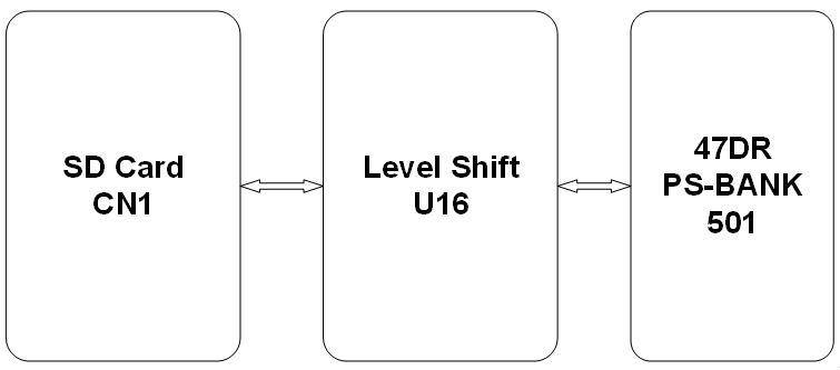
Figure 3.7.1 - Block diagram of PS SD card slot principle
The schematic diagram related to SD is shown in the figure below.
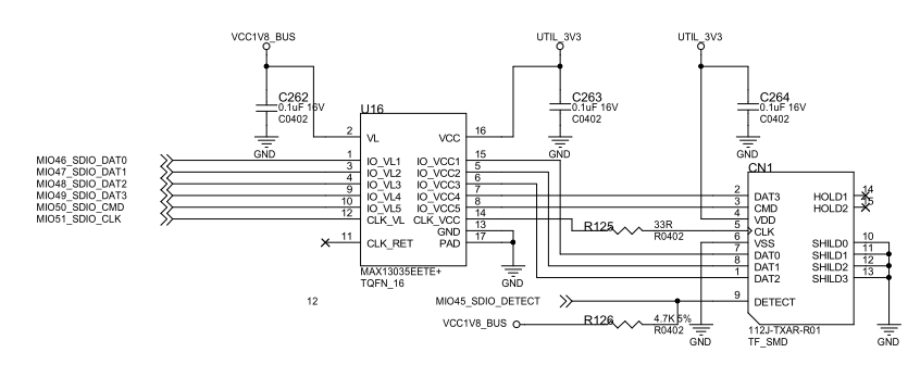
Figure 3.7.2 - Schematic diagram of PS SD card
| 47DR PIN | Schematic Net Name |
| B20 : PS_MIO45_B20 | MIO45_SDIO_DETECT |
| A20 : PS_MIO46_A20 | MIO46_SDIO_DAT0_R |
| D21 : PS_MIO47_D21 | MIO47_SDIO_DAT1_R |
| C21 : PS_MIO48_C21 | MIO48_SDIO_DAT2_R |
| E21 : PS_MIO49_E21 | MIO49_SDIO_DAT3_R |
| A22 : PS_MIO50_A22 | MIO50_SDIO_CMD_R |
| B21 : PS_MIO51_B21 | MIO51_SDIO_CLK_R |
Table 3.7.1 - PS-side SD card pin assignment
3.8 PL I2C Interface
The PL side is connected to an EEPROM via an I2C bus to store some device information. The schematic diagram of this part is shown in the figure below.
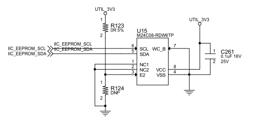
Figure 3.8.1 - Schematic diagram of PL EEPROM principle
| 47DR PIN | Schematic Net Name |
| B10: IO_L2N_AD10N_89_B10 | IIC_EEPROM_SCL |
| C11:IO_L1P_AD11P_89_C11 | IIC_EEPROM_SDA |
Table 3.8.1 - PL-side I2C pin assignment
3.9 PS Ethernet
The board's PS-side Gigabit Ethernet MAC (GEM) can implement a 10/100/1000 Mb/s Ethernet interface, and the PHY chip is a Qualcomm PHY chip . The schematic diagram of this part is shown in the figure below.
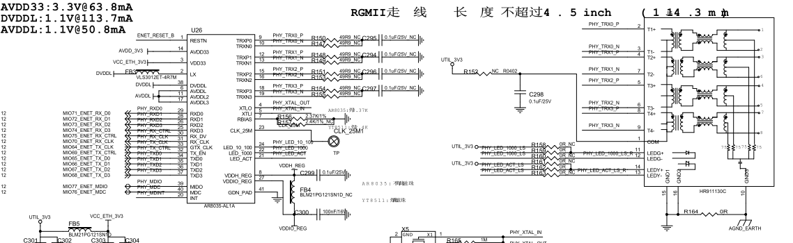
Figure 3.9.1 - Schematic diagram of PS Ethernet principle
| 47DR PIN | Schematic Net Name |
| D26 : PS_MIO77_D26 | MIO77_ENET_MDIO |
| E26 : PS_MIO76_E26 | MIO76_ENET_MDC |
| D24 : PS_MIO64_D24 | MIO64_ENET_TX_CLK |
| E24 : PS_MIO69_E24 | MIO69_ENET_TX_CTRL |
| E25 : PS_MIO68_E25 | MIO68_ENET_TX_D3 |
| F25 : PS_MIO67_F25 | MIO67_ENET_TX_D2 |
| F24 : PS_MIO66_F24 | MIO66_ENET_TX_D1 |
| C24 : PS_MIO65_C24 | MIO65_ENET_TX_D0 |
| B25 : PS_MIO70_B25 | MIO70_ENET_RX_CLK |
| B26 : PS_MIO75_B26 | MIO75_ENET_RX_CTRL |
| C26 : PS_MIO74_C26 | MIO74_ENET_RX_D3 |
| A25 : PS_MIO73_A25 | MIO73_ENET_RX_D2 |
| C25 : PS_MIO72_C25 | MIO72_ENET_RX_D1 |
| A24 : PS_MIO71_A24 | MIO71_ENET_RX_D0 |
| A 23: PS_MIO 60 _A 23 | MIO 60 _ETH_RESET# |
Table 3.9.1 - PS-side Ethernet pin assignment
3.10 JTAG/USB-JTAG
The board can be connected to a JTAG cable via a 14-pin JTAG interface (J4) for debugging the FPGA. A TXS0104EPWR (U18) is used for level conversion (+1.8V to +3.3V) between the JTAG interface and the FPGA, as shown in the diagram below:
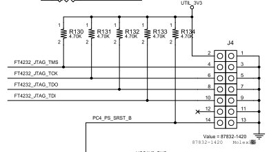
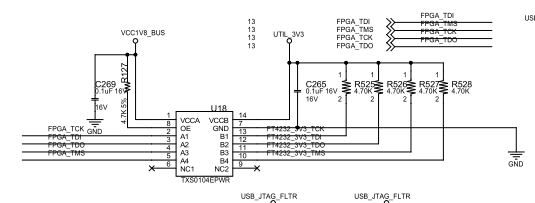
Figure 3.10.1 - Schematic diagram of JTAG interface principle
The board can also debug the FPGA via the TYPEC interface (J3). The USB-JTAG debugging interface is implemented through a dedicated conversion chip FT4232HL (U21), and the principle block diagram is shown in the figure below.
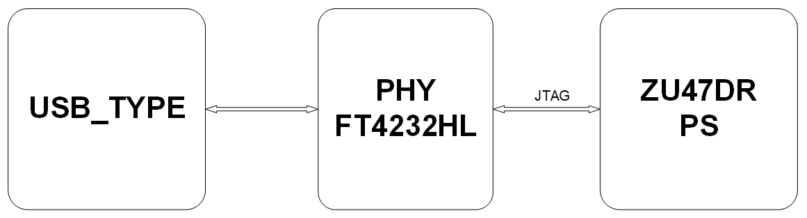
Figure 3.10.2 - USB-JTAG Block Diagram
The schematic diagram of the USB-JTAG part is shown in the figure below.
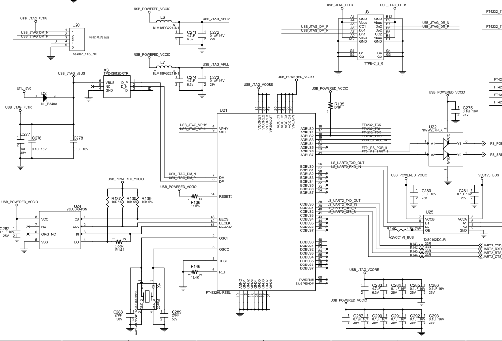
Figure 3.10.3 - Schematic diagram of USB-JTAG interface principle
| 47DR PIN | Schematic Net Name |
| F18: PS_MIO18_F18 | UART0_TXD_MIO18_RXD |
| C16: PS_MIO19_C16 | UART0_RXD_MIO19_TXD |
| B13: IO_L10N_AD10N_88_B13 | UART2_CTS_B |
| C13: IO_L9N_AD11N_88_C13 | UART2_RTS_B |
| C14: IO_L10P_AD10P_88_C14 | UART2_RXD_FPGA_TXD |
| D14:IO_L7N_HDGC_88_D14 | UART2_TXD_FPGA_RXD |
Table 3.10.1 - UART Pin Assignment
3.11 SFP + optical port
This board provides one SFP+ optical port. After level conversion by U31, the SFP+ port interacts with U30 ( SFP + interface) for data exchange. The overall principle block diagram is shown in the figure below.
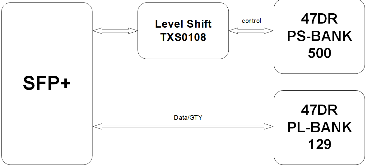
Figure 3.11.1 - Overall block diagram of SFP+ section
The SFP+ schematic diagram is shown below.
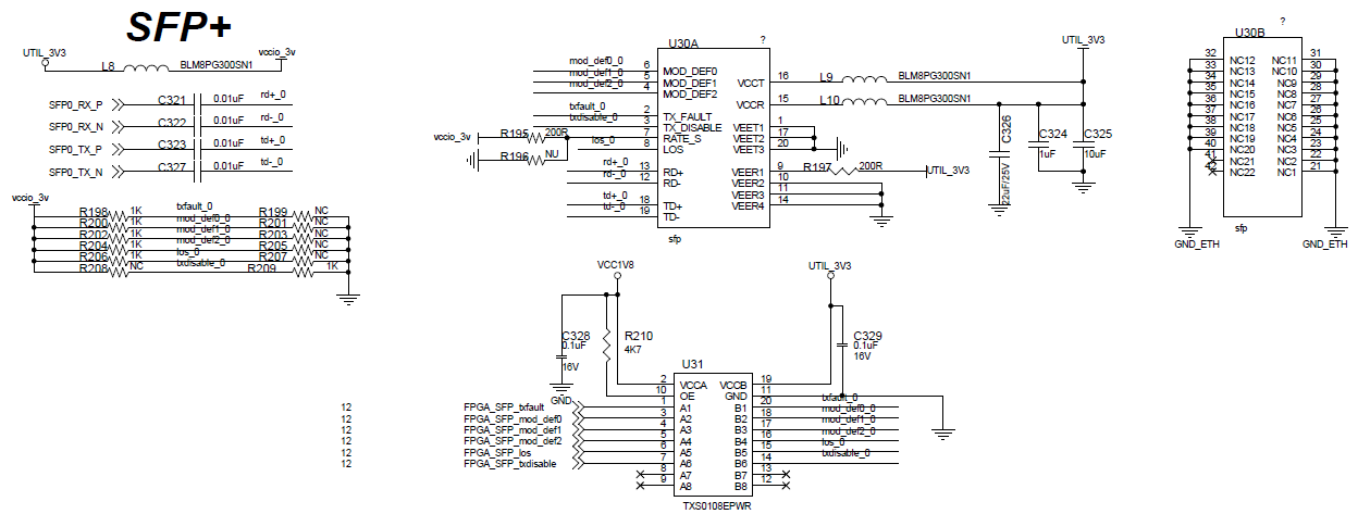
Figure 3.11.2 - SFP+ related schematic diagram
| U31 PIN | Schematic Net Name |
| 1:A1 | FPGA_SFP_txfault |
| 3:A2 | FPGA_SFP_mod_def0 |
| 4:A3 | FPGA_SFP_mod_def1 |
| 5:A4 | FPGA_SFP_mod_def2 |
| 6:A5 | FPGA_SFP_los |
| 7:A6 | FPGA_SFP_txdisable |
Table 3.11.1 - U31 SFP + Control Pin Assignment
| 47DR PIN | Schematic Net Name |
| B17: PS_MIO25_B17 | FPGA_SFP_txfault |
| A17: PS_MIO24_A17 | FPGA_SFP_mod_def0 |
| D17: PS_MIO23_D17 | FPGA_SFP_mod_def1 |
| E17: PS_MIO22_E17 | FPGA_SFP_mod_def2 |
| F17: PS_MIO21_F17 | FPGA_SFP_los |
| B16: PS_MIO20_B16 | FPGA_SFP_txdisable |
| F33: MGTYRXP0_129_F33 | SFP0_RX_P |
| F34: MGTYRXN0_129_F34 | SFP0_RX_N |
| E30: MGTYTXP0_129_E30 | SFP0_TX_P |
| E31: MGTYTXN0_129_E31 | SFP0_TX_N |
Table 3.11.2 - SFP+ Interface Pin Assignment
3.12 QSFP+ Optical Port
This board provides one QSFP+ optical port. After level conversion by U3 , the QSFP + interface interacts with U2 (QSFP+ interface) for data exchange. The overall principle block diagram is shown in the figure below.
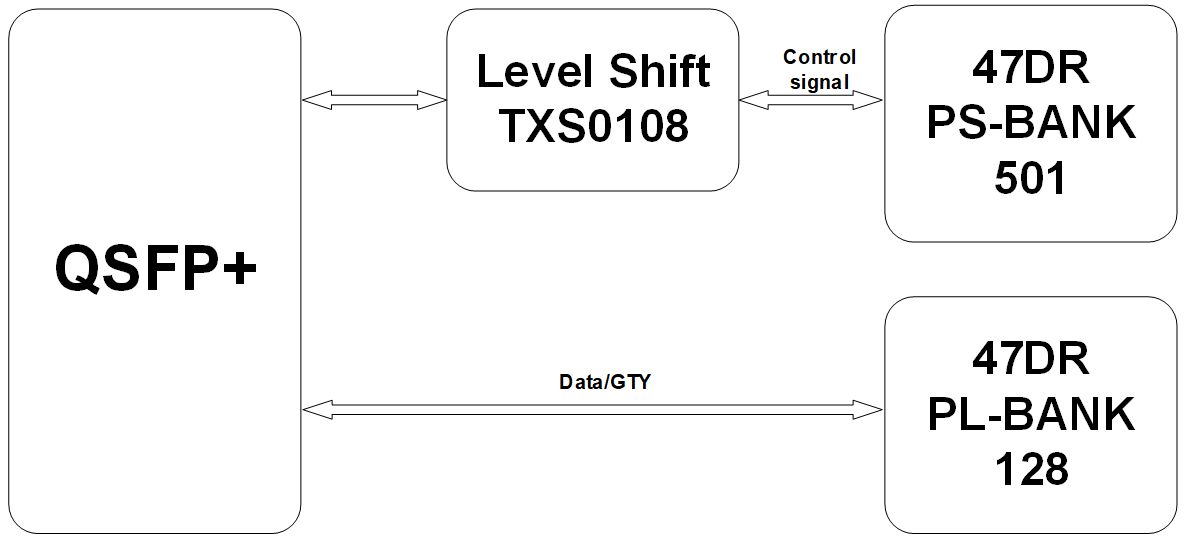
Figure 3.12.1 - Schematic diagram of the overall block diagram of QSFP+
The QSFP+ schematic is shown in the figure below.
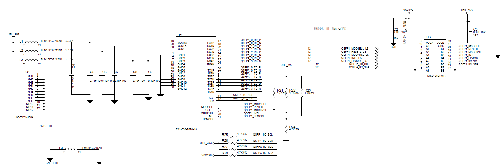
Figure 3.12.2 - QSFP+ related schematic diagram
| U3 PIN | Schematic Net Name |
| 1:A1 | QSFP1_MODSELL_LS |
| 3:A2 | QSFP1_RESETL_LS |
| 4:A3 | QSFP1_MODPRSL_LS |
| 5:A4 | QSFP1_INTL_LS |
| 6:A5 | QSFP1_LPMODE_LS |
| 7:A6 | QSFPA_IIC_SCL |
| 8:A7 | QSFPA_IIC_SDA |
Table 3.12.1 - U3 QSFP+ Control Pin Assignment
| 47DR PIN | Schematic Net Name |
| D19: PS_MIO39_D19 | QSFP1_MODSELL_LS |
| B18 : PS_MIO38_B18 | QSFP1_RESETL_LS |
| E19 : PS_MIO 37 _ E19 | QSFP1_MODPRSL_LS |
| C18 : PS_MIO 36 _ C18 | QSFP1_INTL_LS |
| F20 : PS_MIO 35 _ F20 | QSFP1_LPMODE_LS |
| H20 : PS_MIO 30 _ H20 | QSFPA_IIC_SCL |
| G20 : PS_MIO 31 _ G20 | QSFPA_IIC_SDA |
| P33: MGTYRXP0_128_P33 | QSFPA_0_RD_P |
| P34: MGTYRXN0_128_P34 | QSFPA_0_RD_N |
| M33: MGTYRXP1_128_M33 | QSFPA_1_RD_P |
| M34: MGTYRXN1_128_M34 | QSFPA_1_RD_N |
| K33: MGTYRXP2_128_K33 | QSFPA_2_RD_P |
| K34: MGTYRXN2_128_K34 | QSFPA_2_RD_N |
| H33: MGTYRXP3_128_H33 | QSFPA_3_RD_P |
| H34: MGTYRXN3_128_H34 | QSFPA_3_RD_N |
| N30: MGTYTXP0_128_N30 | QSFPA_0_TD_P |
| N31: MGTYTXN0_128_N31 | QSFPA_0_TD_N |
| L30: MGTYTXP1_128_L30 | QSFPA_1_TD_P |
| L31: MGTYTXN1_128_L31 | QSFPA_1_TD_N |
| J30: MGTYTXP2_128_J30 | QSFPA_2_TD_P |
| J31: MGTYTXN2_128_J31 | QSFPA_2_TD_N |
| G30: MGTYTXP3_128_G30 | QSFPA_3_TD_P |
| G31: MGTYTXN3_128_G31 | QSFPA_3_TD_N |
| M28: MGTREFCLK0P_128_M28 | QSFP_CLK_1_C_P |
| M29: MGTREFCLK0N_128_M29 | QSFP_CLK_1_C_N |
Table 3.12.2 - QSFP+ Interface Pin Assignment
3.13 PL-RS232
The AXW22 XCZU47DR expands one pair of general-purpose I/O ports on the PL side of the BANK89 to create one RS232 interface for external communication, debugging, and printing. The RS232 transceiver chip uses a Maxim Integrated RS232 interface chip. The overall block diagram of this part is shown in the figure below.

Figure 3.13.1 - Overall block diagram of RS232 section
The schematic diagram for the RS232 section is shown in the figure below.
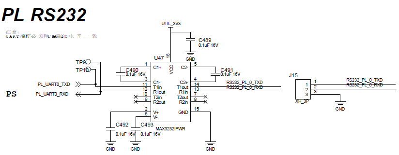
Figure 3.13.2 - Schematic diagram of RS232 part of the circuit.
| 47DR PIN | Schematic Net Name |
| C10: IO_L2P_AD10P_89_C10 | PL_UART0_TXD |
| C9 : IO_L4N_AD8N_89_C9 | PL_UART0_RXD |
Table 3.13.1 - PL-RS232 Interface Pin Assignment
3.14 PL- GPIOX36
The AXW22 directly expands GPIO ports via BANK 88 & 89 on the PL side of the XCZU47DR. Simultaneously, BANK 65 & 66 on the PL side first convert the 1.2V to 3.3V for the IO ports via level converters U34 & U35, then bring them out through connector J8. The 47DR provides abundant expansion IO resources , which can be used to expand IO ports. The block diagram of this part is shown below.
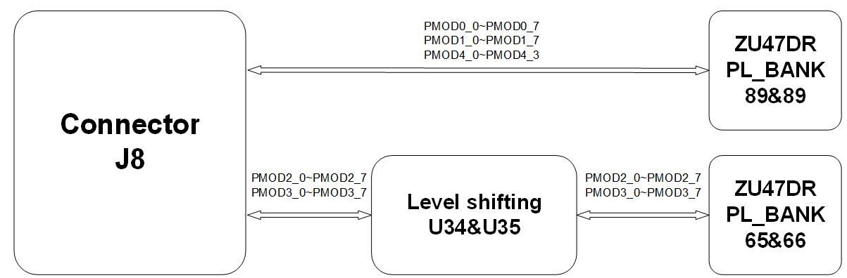
Figure 3.14.1 - GPIO X 36 Principle Block Diagram
The circuit diagram for this part is shown in the figure below.
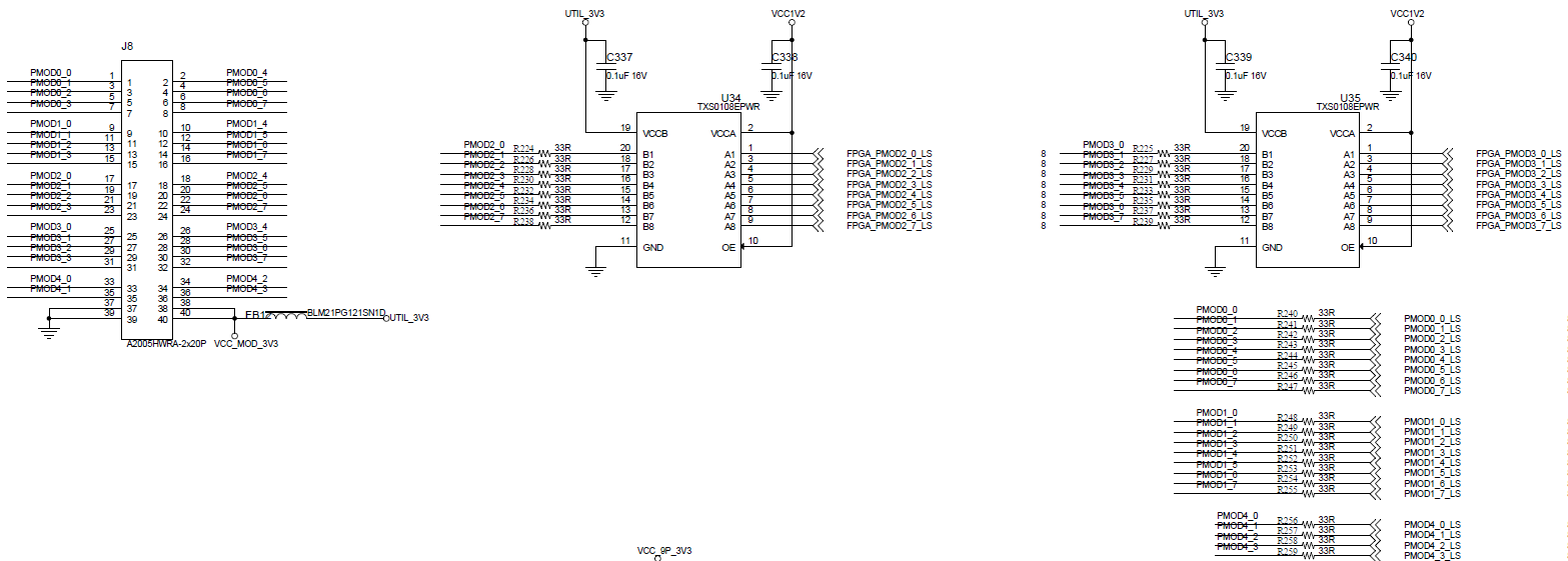
Figure 3.14.2 - Schematic diagram of GPIOX36 principle
| 4 7DR PIN | Schematic Net Name | J8 | |
| Pin Number | Pin Net Name | ||
| J13 : IO_L3N_AD13N_88_J13 | PMOD0_0_LS | 1 | PMOD0_0 |
| K14 : IO_L1N_AD15N_88_K14 | PMOD0_1_LS | 3 | PMOD0_1 |
| J14 : IO_L3P_AD13P_88_J14 | PMOD0_2_LS | 5 | PMOD0_2 |
| H1 5: IO_L2P_AD14P_88_H15 | PMOD0_3_LS | 7 | PMOD0_3 |
| H14: IO_L2N_AD14N_88_H14 | PMOD0_4_LS | 2 | PMOD0_4 |
| K15 : IO_L1P_AD15P_88_K15 | PMOD0_5_LS | 4 | PMOD0_5 |
| F13: IO_L5N_HDGC_88_F13 | PMOD0_6_LS | 6 | PMOD0_6 |
| F14: IO_L5P_HDGC_88_F14 | PMOD0_7_LS | 8 | PMOD0_7 |
| E14 : IO_L7P_HDGC_88_E14 | PMOD1_0_LS | 9 | PMOD1_0 |
| D13 : IO_L9P_AD11P_88_D13 | PMOD1_1_LS | 11 | PMOD1_1 |
| A1 4: IO_L11P_AD9P_88_A14 | PMOD1_2_LS | 13 | PMOD1_2 |
| F12: IO_L6N_HDGC_88_F12 | PMOD1_3_LS | 15 | PMOD1_3 |
| K12: IO_L12P_AD0P_89_K12 | PMOD1_4_LS | 10 | PMOD1_4 |
| A13: IO_L11N_AD9N_88_A13 | PMOD1_5_LS | 12 | PMOD1_5 |
| J12: IO_L12N_AD0N_89_J12 | PMOD1_6_LS | 14 | PMOD1_6 |
| G12: IO_L6P_HDGC_88_G12 | PMOD1_7_LS | 16 | PMOD1_7 |
| AH12 : IO_T3U_N12_66_AH12 | FPGA_PMOD2_0_LS | 17 | PMOD2_0 |
| AJ12 : IO_T2U_N12_66_AJ12 | FPGA_PMOD2_1_LS | 19 | PMOD2_1 |
| AN1 : IO_L6N_T0U_N11_AD6N_66_AN1 | FPGA_PMOD2_2_LS | 21 | PMOD2_2 |
| AN2 : IO_L6P_T0U_N10_AD6P_66_AN2 | FPGA_PMOD2_3_LS | 23 | PMOD2_3 |
| A P2: IO_L5N_T0U_N9_AD14N_66_AP2 | FPGA_PMOD2_4_LS | 18 | PMOD2_4 |
| A P3: IO_L5P_T0U_N8_AD14P_66_AP3 | FPGA_PMOD2_5_LS | 20 | PMOD2_5 |
| AN 4: IO_L4N_T0U_N7_DBC_AD7N_66_AN4 | FPGA_PMOD2_6_LS | 22 | PMOD2_6 |
| A M5: IO_L3N_T0L_N5_AD15N_66_AM5 | FPGA_PMOD2_7_LS | 24 | PMOD2_7 |
| AD17 : IO_T3U_N12_65_AD17 | FPGA_PMOD3_0_LS | 25 | PMOD3_0 |
| AD13 : IO_L19N_T3L_N1_DBC_AD9N_65_AD13 | FPGA_PMOD3_1_LS | 27 | PMOD3_1 |
| AG16 : IO_T2U_N12_65_AG16 | FPGA_PMOD3_2_LS | 29 | PMOD3_2 |
| AH15 : IO_L13N_T2L_N1_GC_QBC_65_AH15 | FPGA_PMOD3_3_LS | 31 | PMOD3_3 |
| AL16 : IO_T1U_N12_65_AL16 | FPGA_PMOD3_4_LS | 26 | PMOD3_4 |
| AJ13 : IO_L7N_T1L_N1_QBC_AD13N_65_AJ13 | FPGA_PMOD3_5_LS | 28 | PMOD3_5 |
| AN14 : O_L1N_T0L_N1_DBC_65_AN14 | FPGA_PMOD3_6_LS | 30 | PMOD3_6 |
| AP8 : IO_L1P_T0L_N0_DBC_66_AP8 | FPGA_PMOD3_7_LS | 32 | PMOD3_7 |
| K10: IO_L10N_AD2N_89_K10 | PMOD4_0_LS | 33 | PMOD4_0 |
| H9: IO_L9N_AD3N_89_H9 | PMOD4_1_LS | 35 | PMOD4_1 |
| H1 0: IO_L9P_AD3P_89_H10 | PMOD4_2_LS | 34 | PMOD4_2 |
| F9: IO_L7N_HDGC_AD5N_89_F9 | PMOD4_3_LS | 36 | PMOD4_3 |
Table 3.14.1 - GPIO X 36 Pin Assignment and Correspondence with J2
3.15 PL-USER LED
The AXW22 uses the BANK66 on the PL side of the XCZU47DR and a U39 level converter chip to convert 8 GPIO ports from 1.2V to 3.3V, then connects to 8 LEDs for user development. This part of the interface circuit is shown below.
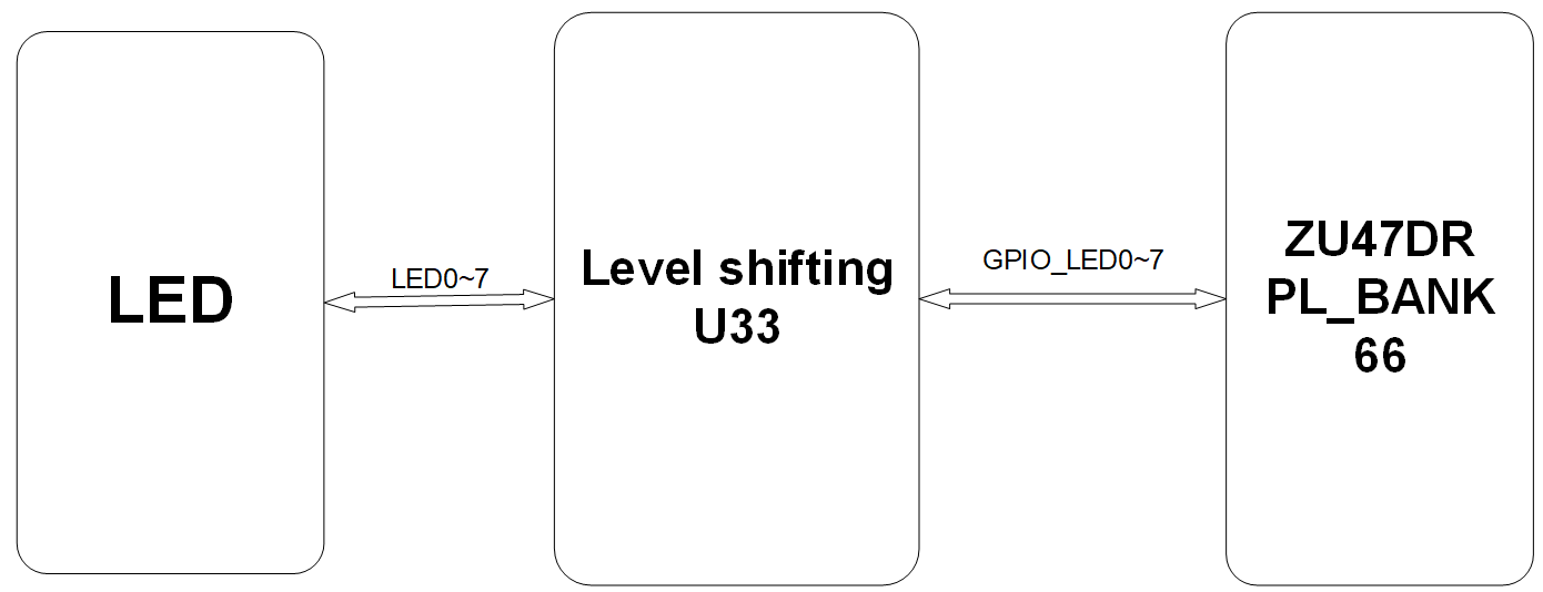
Figure 3.15.1 - USER-LED Interface Circuit
The schematic diagram of this circuit is shown in the figure below.
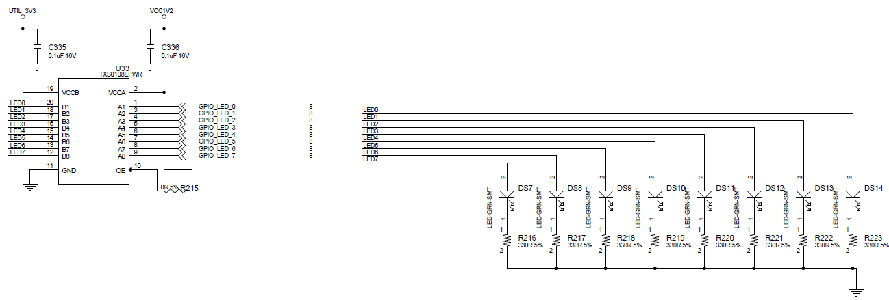
Figure 3.15.2 - Schematic diagram of USER-LED circuit principle
| 47DR PIN | Schematic Net Name |
| AP 5: IO_L2N_T0L_N3_66_AP5 | GPIO_LED_0 |
| AN5 : IO_L4P_T0U_N6_DBC_AD7P_66_AN5 | GPIO_LED_1 |
| A P6: IO_L2P_T0L_N2_66_AP6 | GPIO_LED_2 |
| AM6 : IO_L3P_T0L_N4_AD15P_66_AM6 | GPIO_LED_ 3 |
| A P7: IO_L1N_T0L_N1_DBC_66_AP7 | GPIO_LED_4 |
| A M7: IO_L10N_T1U_N7_QBC_AD4N_66_AM7 | GPIO_LED_5 |
| AM 8: IO_L10P_T1U_N6_QBC_AD4P_66_AM8 | GPIO_LED_ 6 |
| A N9: IO_T1U_N12_66_AN9 | GPIO_LED_ 7 |
Table 3.15.1 - PL-USER LED Interface Pin Assignment
3.16 PL-SPI Interface
The AXW22 outputs one SPI interface via the BANK89 on the PL side of the XCZU47DR, and also reserves one GPIO port. All I/O levels are 3.3V, for user development purposes. The interface circuitry is as follows.
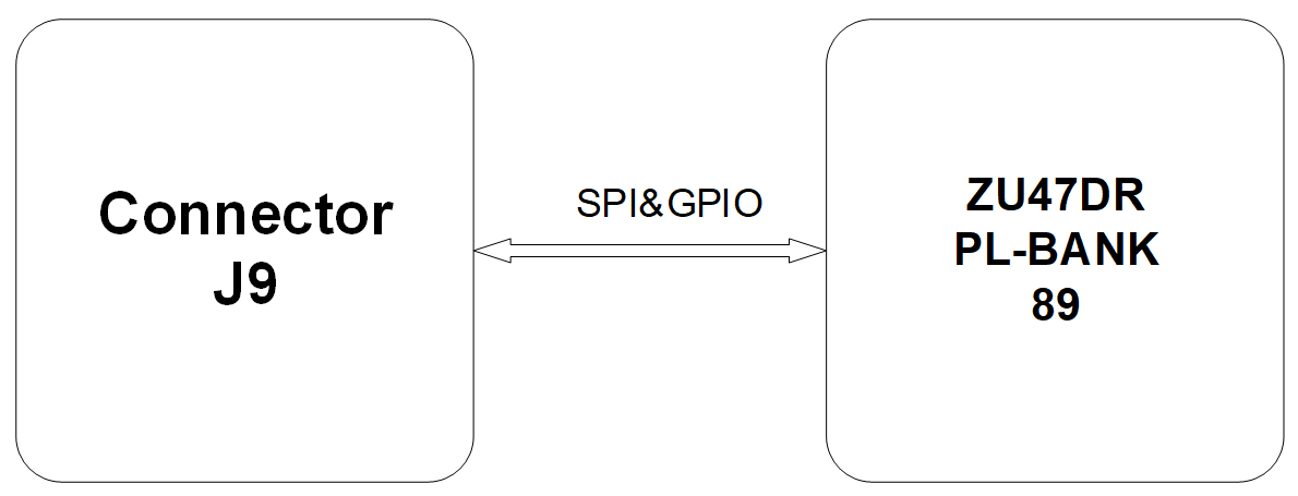
Figure 3.16.1 - SPI Interface Block Diagram
The schematic diagram of this circuit is shown in the figure below.
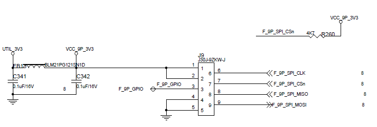
Figure 3.16.2 - Schematic diagram of SPI interface principle
| 47DR PIN | Schematic Net Name |
| F10 : IO_L7P_HDGC_AD5P_89_F10 | F_9P_SPI_CLK |
| H11 : IO_L11N_AD1N_89_H11 | F_9P_SPI_CSn |
| E11 : IO_L5P_HDGC_AD7P_89_E11 | F_9P_SPI_MISO |
| D11 : IO_L5N_HDGC_AD7N_89_D11 | F_9P_SPI_MOSI |
| J11 : IO_L11P_AD1P_89_J11 | F_9P_GPIO |
Table 3.16.1 - PL- SPI Interface Pin Assignment
3.17 PL - SMA-GPIO
The AXW22 outputs one GPIO through the BANK89 on the PL side of the XCZU47DR via the SMA interface. The IO level is 3.3V and it is used for external triggering.
| 47DR PIN | Schematic Net Name |
| K11: IO_L10P_AD2P_89_K11 | PL_JHD_P |
Table 3.17.1 - PL -SMA-GPIO Interface Pin Assignment
3.18 GPS Module
AXW22 connects to an external GPS module via a pair of GPIO ports on the PL side of the XCZU47DR , with a side-mounted SMA interface. The overall block diagram is shown below.
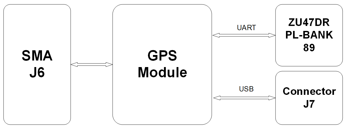
Figure 3.18.1 - Overall block diagram of the GPS section
The schematic diagram for this part is shown below.
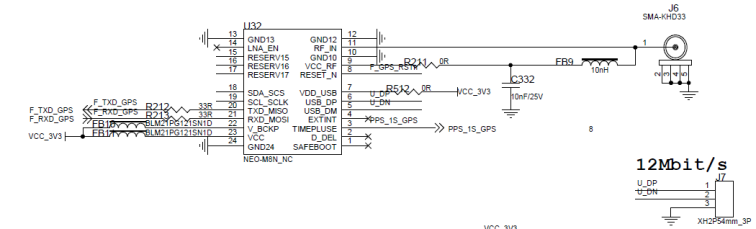
Figure 3.18.2 - Schematic diagram of GPS principle
| 47DR PIN | Schematic Net Name |
| D9 : IO_L4P_AD8P_89_D9 | F_TXD_GPS |
| A9 : IO_L3N_AD9N_89_A9 | F_RXD_GPS |
Table 3.18.1 - GPS Module Pin Assignment
3.19 RF Data Converters
The product supports two 14- bit ADC inputs at 4.096 GSPS and two 14-bit DAC outputs at 6.4 GSPS. The front-end interface is a side-plug SMA, with single-ended signal input and output. Differential-to-single-ended conversion is achieved through a balun device to complete data transmission and reception. The overall block diagram is shown below.
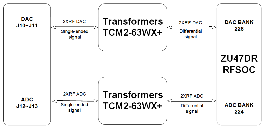
Figure 3.19.1 - Overall block diagram of ADC & DAC interface
The schematic diagram for the main chip ZU47DR and its ADC section is shown in the figure below.

Figure 3.19.2 - Schematic diagram of ADC interface principle
The schematic diagram for the main chip ZU47DR and its DAC section is shown in the figure below.
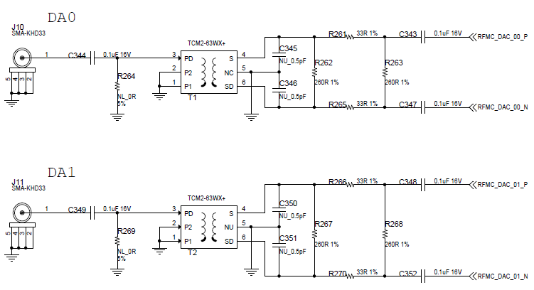
Figure 3.19.3 - Schematic diagram of DAC interface principle
| 47DR PIN | Schematic Net Name |
| AK2: ADC_VIN_I01_P_224_AK2 | RFMC_ADC_00_P |
| AK1: ADC_VIN_I01_N_224_AK1 | RFMC_ADC_00_N |
| AJ5: VCM01_224_AJ5 | VCM01_224 |
| AJ4: VCM23_224_AJ4 | VCM23_224 |
| AD5: ADC_CLK_P_224_AD5 | RF_CLK_224_C_P |
| AD4: ADC_CLK_N_224_AD4 | RF_CLK_224_C_N |
| A H 2: ADC_VIN_I23_P_224_AH2 | RFMC_ADC_01_P |
| A H 1: ADC_VIN_I23_N_224_AH1 | RFMC_ADC_01_N |
| AH5: VCM01_225_AH5 | VCM01_225 |
| AH4: VCM23_225_AH4 | VCM23_225 |
| AG5: VCM01_226_AG5 | VCM01_226 |
| AG4: VCM23_226_AG4 | VCM23_226 |
| AF5: VCM01_227_AF5 | VCM01_227 |
| AF4: VCM23_227_AF4 | VCM23_227 |
| N2: DAC_VOUT0_P_228_N2 | RFMC_DAC_00_P |
| N1: DAC_VOUT0_N_228_N1 | RFMC_DAC_00_N |
| J2: DAC_VOUT2_P_228_J2 | RFMC_DAC_01_P |
| J1: DAC_VOUT2_N_228_J1 | RFMC_DAC_01_N |
| N5: SYSREF_P_228_N5 | SYSREF_RFSOC_C_P |
| N4: SYSREF_N_228_N4 | SYSREF_RFSOC_C_N |
| L5: DAC_CLK_P_228_L5 | RF_CLK_228_C_P |
| L4: DAC_CLK_N_228_L4 | RF_CLK_228_C_N |
Table 3.19.1 - AD and DA Interface Pin Assignments
Appendix: List of Abbreviations
| Abbreviation | Full English Name | Description |
| PS | Processor System | The processing subsystem in an SoC, typically including CPU cores, memory controllers, and peripheral interfaces for running software and operating systems. |
| PL | Programmable Logic | User-configurable FPGA logic resources used to implement custom digital circuits, interface controllers, and hardware acceleration functions. |
| SOC | System on Chip | An integrated circuit that combines processors, memory controllers, peripheral interfaces, and other system functions on a single chip. |
| DDR3 | Double Data Rate 3 SDRAM | A third-generation synchronous dynamic memory technology that transfers data on both edges of the clock signal and is commonly used as system memory. |
| eMMC | Embedded Multi Media Card | An embedded non-volatile storage device that integrates NAND Flash memory and a storage controller in a single package. |
| QSPI | Quad Serial Peripheral Interface | A high-speed serial interface that uses four data lines and is commonly used to connect NOR Flash devices for boot or configuration storage. |
| GTP | Gigabit Transceiver | A high-speed serial transceiver integrated in an FPGA for transmitting and receiving data at multi-gigabit rates. |
| UART | Universal Asynchronous Receiver/Transmitter | An asynchronous serial communication interface that transmits and receives data through TX and RX signal lines. |
| HDMI | High-Definition Multimedia Interface | A digital multimedia interface used to transmit high-definition video and audio signals between source and display devices. |
| PCIe | Peripheral Component Interconnect Express | A high-speed serial expansion bus standard used for communication between processors and devices such as FPGAs, GPUs, and SSDs. |
| USB | Universal Serial Bus | A standard serial interface used for data communication, peripheral connection, and power delivery between electronic devices. |
| JTAG | Joint Test Action Group | A standardized interface used for device testing, boundary scan, FPGA programming, and processor or system debugging. |
| SFP | Small Form-factor Pluggable | A compact, hot-pluggable transceiver interface used for optical or electrical network communication. |
| MIO | Multiplexed I/O | Multiplexed processor I/O pins in an SoC that can be configured for functions such as UART, I2C, SPI, or GPIO. |
| GPHY | Gigabit Ethernet PHY | A Gigabit Ethernet physical-layer transceiver that converts digital Ethernet data into electrical signals for transmission over a physical network medium. |
| I2C | Inter-Integrated Circuit | A two-wire serial communication bus using SDA and SCL lines, commonly used to connect sensors, EEPROMs, and peripheral devices. |
| RGMII | Reduced Gigabit Media Independent Interface | A reduced-pin-count interface between an Ethernet MAC and PHY that supports 10, 100, and 1000 Mbps Ethernet communication. |
| RMII | Reduced Media Independent Interface | A reduced-pin-count interface between an Ethernet MAC and PHY, mainly used for 10 and 100 Mbps Ethernet communication. |
| LED | Light Emitting Diode | A semiconductor device that emits light when electrically driven and is commonly used for power, status, and fault indication. |
| LVDS | Low-Voltage Differential Signaling | A high-speed differential signaling standard that provides low power consumption, low noise, and strong resistance to electromagnetic interference. |
Contact information
Alinx Electronic Limited
Company Website: www.en.alinx.com
Service Hotline: +86 21 67676997
Technical Support:technical@alinx.com