
Appearance
AXW49 User Manual

Alinx Electronic Limited
Company Website: www.en.alinx.com
Service Hotline: +86 21 67676997
Technical Support : technical@alinx.com
Document Information
| Item | Content |
| Document Name | Product Manual |
| Product Model | AXW49 |
| Document Version | V1.0 |
| Prepared by | Alinx Electronic Limited |
| Release Date | 2026.9.24 |
Document Revision History
| Version | Date | Section | Revision Summary |
| V1.0 | 2026.9.24 | All | Initial Release |
Part 1:Introduction
1.1 Product Description
The ZYNQ chip in the ZU49DR_COME is based on Xilinx's Zynq™ UltraScale+™ RFSoC Gen3 series XCZU49DR-2FFVF1760E. It also incorporates a Kontron x86 COME module to provide superior data processing performance.
The ZU49DR_COME uses eight Micron MT40A512M16HA DDR4 chips. Four DDR4 chips are connected to the PS side, forming a 64-bit data bus, and four DDR4 chips are connected to the PL side, also forming a 64-bit data bus. The maximum operating data rate of the DDR4 SDRAM is 2400Mb/s. The board also integrates two 1Gb QSPI FLASH chips for boot storage configuration and system files.It also expands to one M.2 NVMe port for high-performance data processing and storage, and another SD card slot for storing file systems and other user data files. The ZU49DR_COME has two onboard 100Gbps QSFP28 connectors for optical ports, enabling efficient high-speed data processing in parallel with analog and digital conversion. The PS side expands to one USB 3.0 port, and both the PS and PL sides each expand to one 10/100/1000 Ethernet port. This board expands to include one USB 3.0 port , one RJ45 port, one video interface, and one embedded storage chip via board-to-board connector U21 .
The ZU49DR_COME board features 16 ADC and 16 DAC ports. The ZU49DR_COME with the ZU49DR FPGA is powered by 16 14-bit 2.5 GSPS ADC ports and 16 14-bit 9.85 GSPS DAC ports. The ADC and DAC ports utilize the high-performance miniature RF connector 190-0108-AAD1.
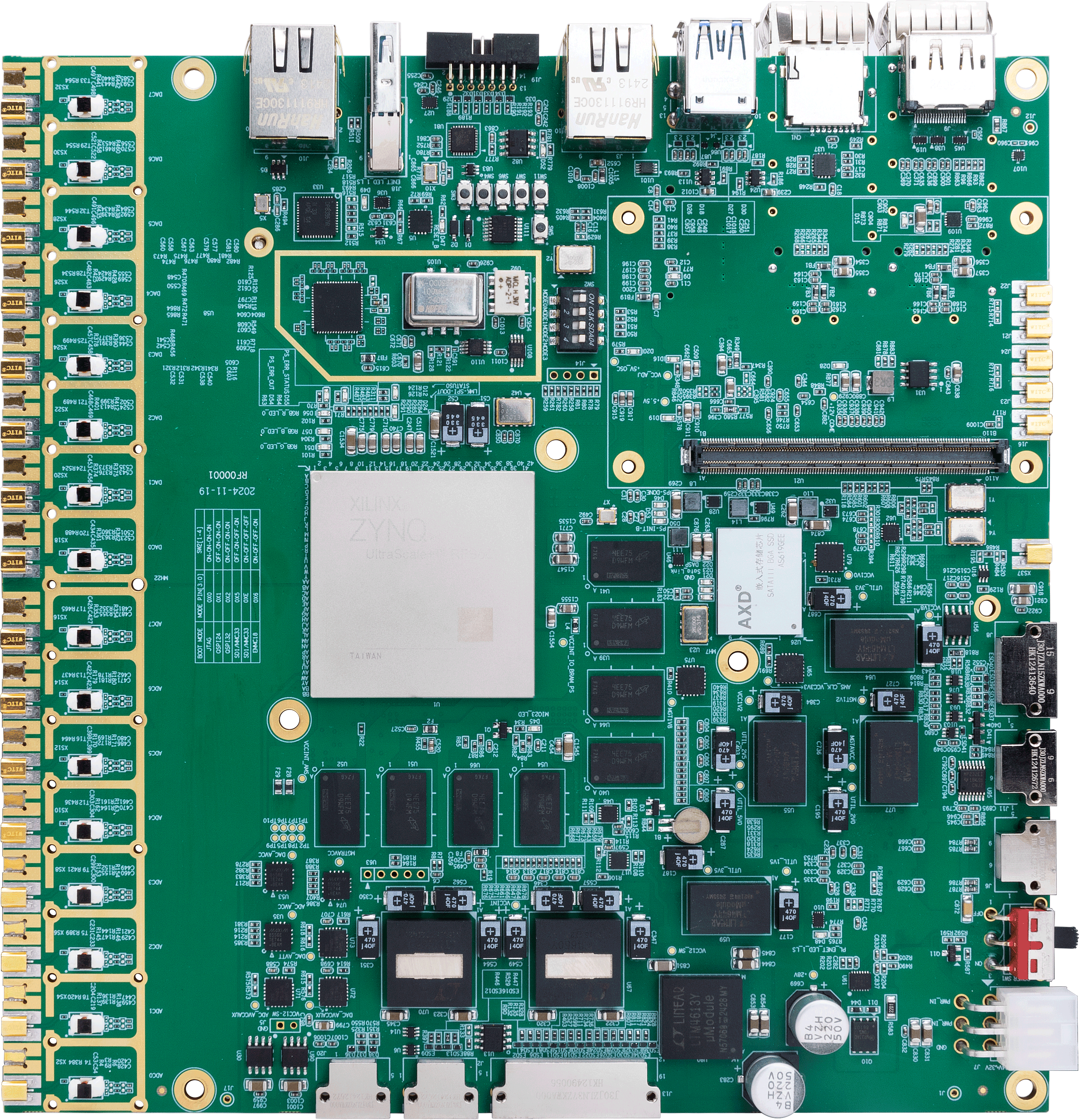
Figure 1.1.1 - Front view of ZU49DR_COME
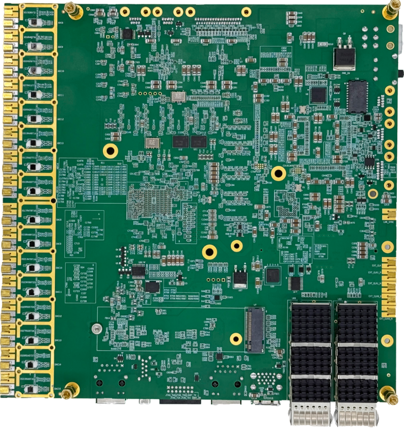
Figure 1.1.2 - Back of ZU49DR_COME
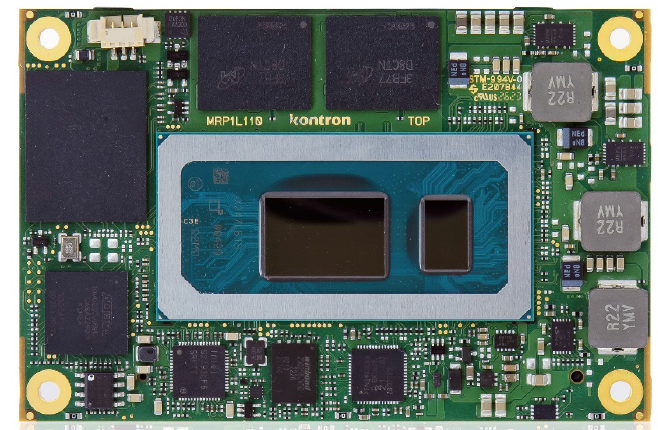
Figure 1.1.3 - COME Module Diagram
1.2 ZYNQ Chip
The ZU49DR_COME utilizes a Xilinx Zynq™ UltraScale+™ RFSoC Gen3 series chip, model XCZU49DR-2FFVF1760E. The FPGA resources in the programmable logic section provide high-throughput digital signal processing (DSP) and IP cores, such as digital up/down conversion (DUC/DDC) cores. FPGA acceleration is easier to implement through the software-defined radio development architecture application programming interface and FPGA infrastructure. This facilitates rapid startup and operation, allowing focus on value-added IP. FPGA systems for commonly used functions such as Fast Fourier Transform (FFT) and Finite Impulse Response (FIR) filters are a good starting point. Users can add their own IP blocks to modular architecture using their preferred Hardware Description Language (HDL). In addition to the FPGA architecture portion of the system, the Xilinx UltraScale+ RFSoC also features four onboard Application Processing Units (APUs) and two Real-Time Processing Units (RPUs), suitable for applications requiring independent operation of an onboard embedded operating system.
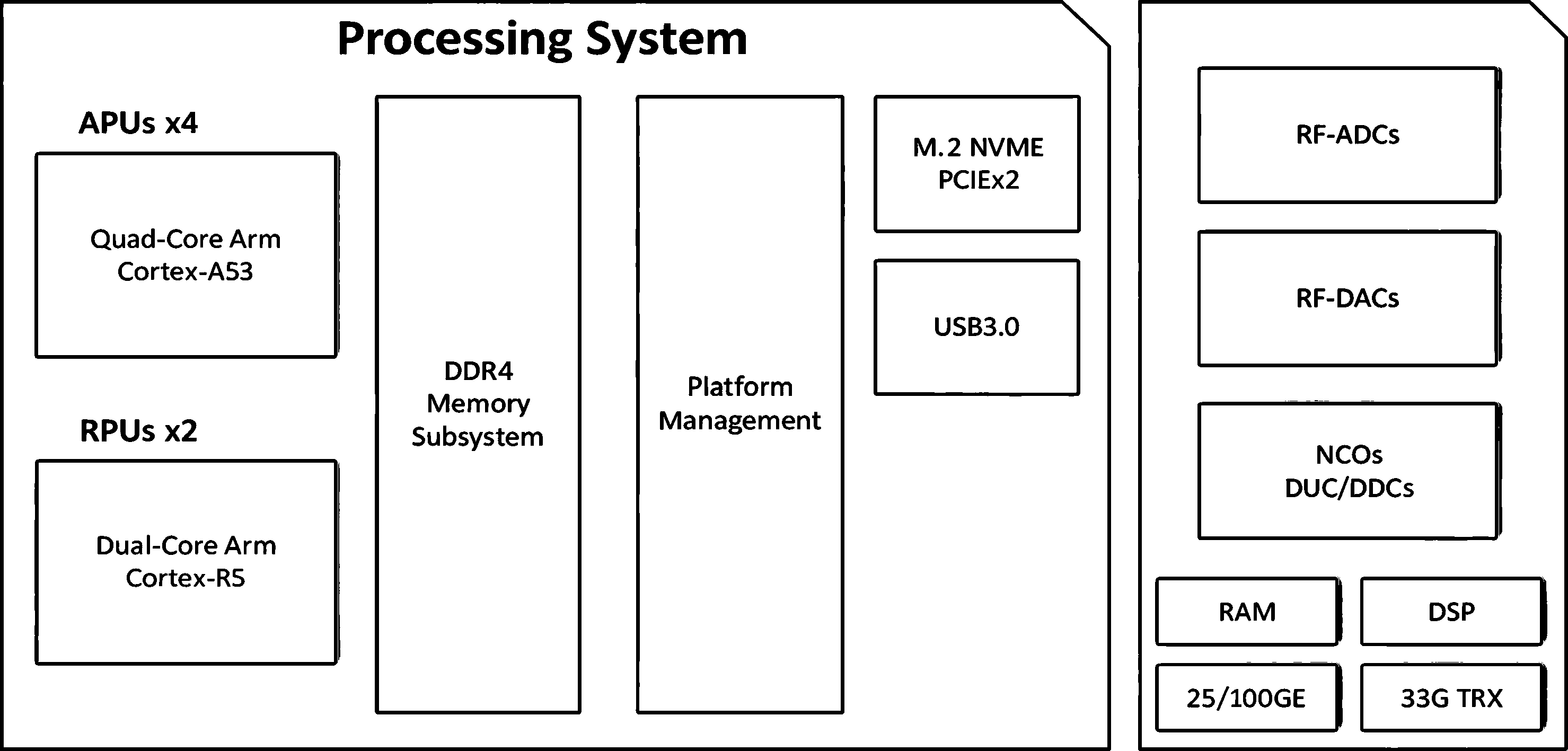
Figure 1.2.1 - RFSOM System Block Diagram
1.3 Product Features
Maximize input/output channel density
It supports 16 channels of 14-bit RF-ADC and 16 channels of 14-bit RF-DAC, providing a comprehensive RF signal chain to maximize input/output channel density, high bandwidth, heterogeneous processing capabilities, and low power consumption. It can synchronize all 16 channels and multiple boards to meet the needs of larger system applications .
Reduce RF signal chain complexity
Radar and EW systems with multiple channels face cost and complexity challenges, as more channels mean more expensive and larger RF signal up/down conversions and signal conditioning. A common solution is direct RF sampling—a more flexible approach than traditional analog frequency conversion and filtering. Direct RF sampling can be implemented in the digital domain, consuming less power and generally being less expensive. This means the RF front end can handle a wider bandwidth than traditional analog techniques while consuming less power. As with RFSoC devices, using very high sampling rates in the data converters means that most of the analog filtering and conditioning can be done closer to the antenna, providing a simpler and more flexible front end than in the past. By integrating the ADC and DAC into the device, the need for the JESD204B is eliminated—simplifying design complexity and helping to reduce latency.
Heterogeneous processing capability
Radar and electronic warfare systems, for example, require streaming DSPs with FPGAs and general-purpose processors for decision-making and control. Previously, these processing requirements were handled by separate modules; now, with the ZU49DR_COME, both functionalities can be integrated into a single module using RFSoC technology. This is particularly relevant to the growing demands of today's smart radar/electronic warfare technologies. Furthermore, the simplified integration with RF sampling devices eliminates the complexity of the JESD204B high-speed serial interface. This means that basic functions such as inter-device communication consume fewer programmable logic elements, resulting in more computational resources available for application-specific IP than before.
1.4 Application Scenarios
Communication application scenarios
5G and LTE wireless technologies: With Zynq RFSoC, wireless infrastructure manufacturers can achieve significant reductions in footprint and power consumption, which is crucial for the development of later MIMO technologies.
Satellite communications: Designers can build high-speed, multi-functional instruments for signal generation and analysis by utilizing direct RF sampling, highly flexible, reconfigurable logic, and software programmability in the Zynq UltraScale+ RFSoC.
Radar application scenarios
Radar signal processing and data link: Equipped with a 16-channel ADC and a 16-channel DAC, it can meet greater application requirements and achieve low-latency transmission and reception in early warning scenarios, thus obtaining the best response time.
Test and Measurement Application Scenarios
Designers can leverage RF sampling, highly flexible, reconfigurable logic, and software programmability in the Zynq UltraScale+ RFSoC to build high-speed, multi-functional instruments for signal generation and analysis.
Part 2:Platform Hardware Introduction
2.1 Hardware Block Diagram
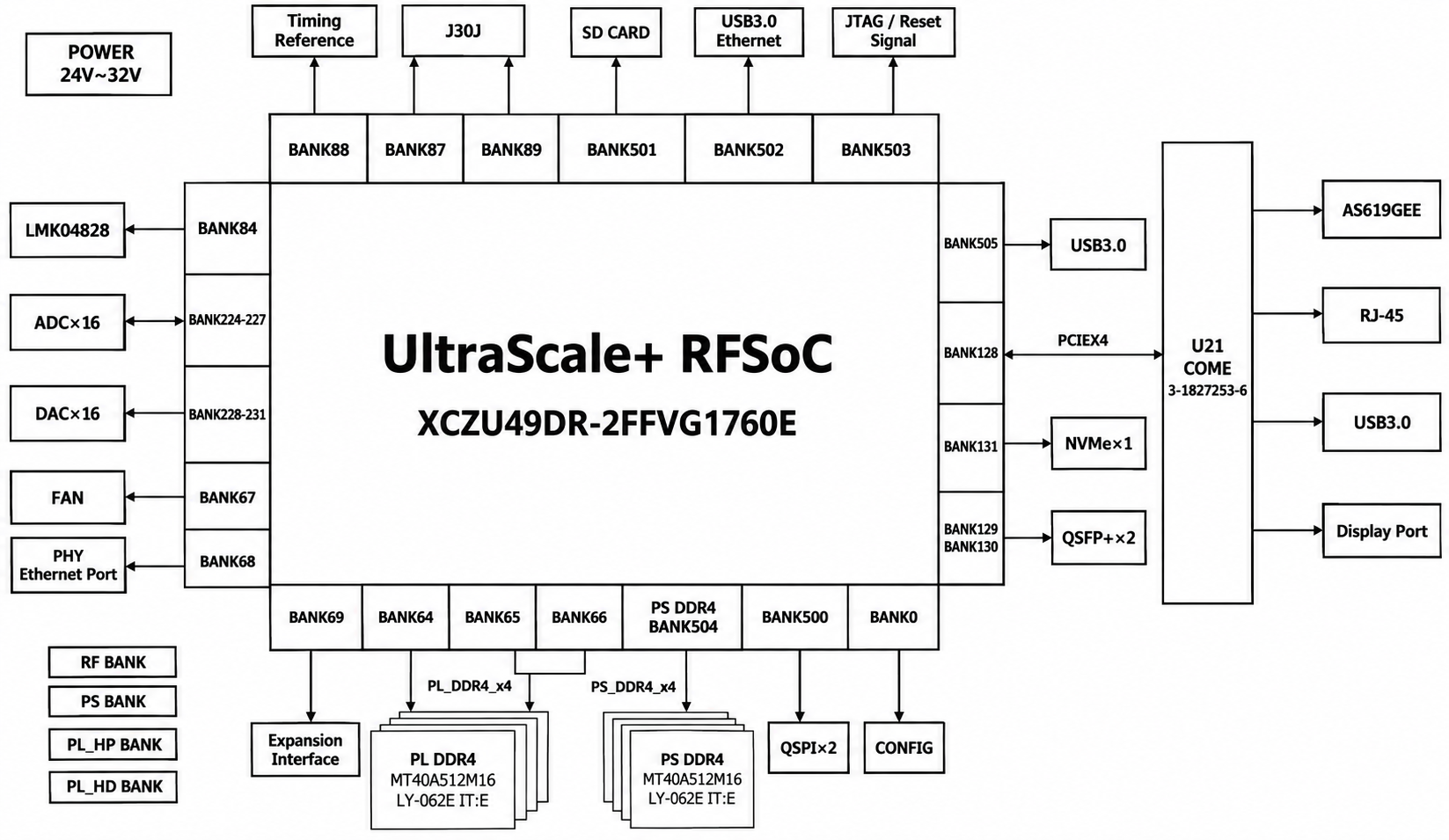
Figure 2.1.1 - Block diagram of ZU49DR_COME board
2.2 Main Specifications
| Technical parameters | |
| FPGA chip | Zynq UltraScale+ XCZU49DR-2FFVF1760E |
| RF interface | 1. X16ADC (14-bit, 2.5GSPS) ports1. X16DAC (14-bit, 9.85GSPS) ports |
| 100G optical port | 2 |
| Interface speed | Supports 100GE*2 |
| M.2 interface | NVMe*1 |
| Memory | PS 4xDDR4(4GB,64bit, 2400MT/s) PL 4xDDR4 (4GB, 64bit, 2400MT/s) |
| Power supply for the board | The power supply interface is 39-30-1060 (input voltage 24~32V). |
| PS interface | 1. 2x QSPI flash (128MB, 8bit) firmware configuration files1. 1 x USB 3.0 Port1. 1 x 10/100/1000 Ethernet RGMII (RJ45) port1. 1 Micro SD Card |
| PL interface | 1. 1x M.2 interface1. 16-channel ADC (14-bit, 2.5GSPS) port1. 16-channel DAC (14-bit, 9.85GSPS) ports1. 2x QSFP 100G optical ports1. 32x IO1. 1 x 10/100/1000 Ethernet RGMII (RJ45) port |
| size | 199.9996mm*199.9996mm |
| Power consumption | 60W (based on actual measured value, depending on the application) |
| Ambient temperature requirements | Operating temperature: -40℃ to 70 ℃ |
| Reference Project | |
| -Configure ADC/DAC related registers in the host computer software High-speed ADC/DAC loopback testing engineering - Schematics (.pdf format) - DDR4 Reference Design - FPGA Pin Arrangement | |
2.3 Functions and locations of the circuit board
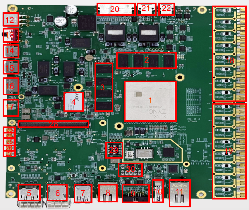
Figure 2.3.1 - ZU49DR_COME board physical TOP
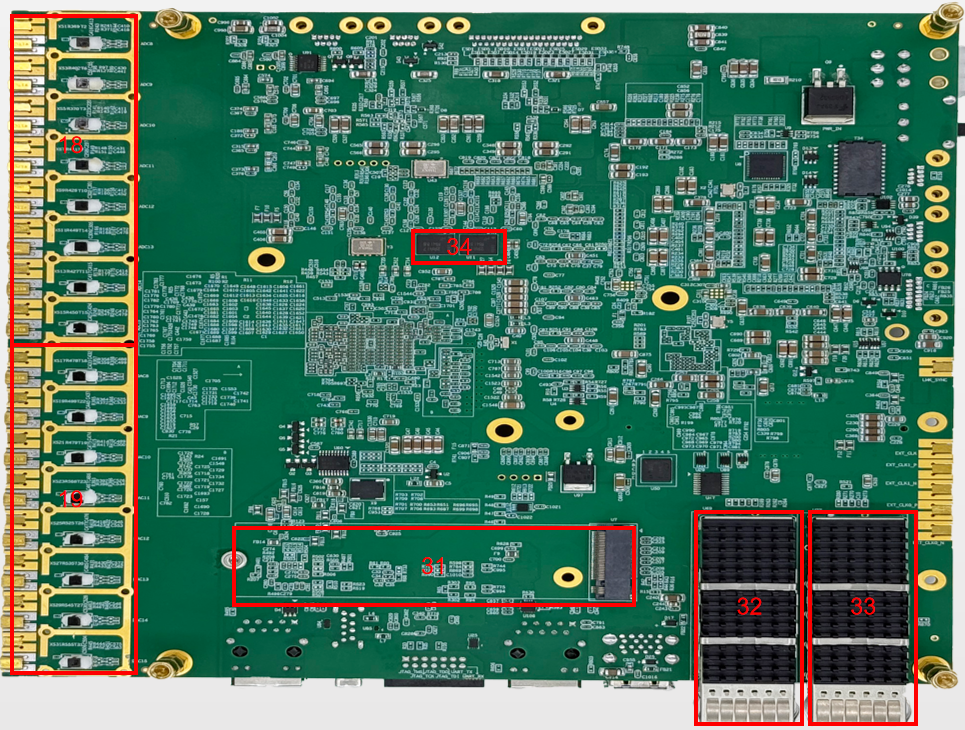
Figure 2.3.2 - ZU49DR_COME board physical BOTTOM
| Serial Number | Location | Function |
| 1 | U1 | XCZU49DR-2FFVF1760E |
| 2 | U51, U52, U54, U66 | PL side DDR4 |
| 3 | U39, U40, U41, U44 | PS side DDR4 |
| 4 | U26 | COME-inspired memory chips |
| 5 | J9 | COME introduces the Display Port |
| 6 | CN1 | SD card slot |
| 7 | J4 | The USB 3.0 interface brought out by COME |
| 8 | J3 | Gigabit Ethernet Port from COME |
| 9 | J19 | JTAG debug port |
| 10 | J18 | PS-side USB 3.0 interface |
| 11 | J10 | PS terminal gigabit network port |
| 12 | J7 | Power input |
| 13 | SW1 | power switch |
| 14 | J6 | PL port |
| 15 | J11 | Expansion interface (J30JZLN09ZKW) |
| 16 | J8 | Expansion interface (J30JZLN15ZKW) |
| 17 | XS37 | LMK_SYNC |
| 18 | XS1~XS16 | ADC0~ADC15 |
| 19 | XS17~XS32 | DAC0~DAC15 |
| 20 | J13 | Extended I/O (J30JZLN37ZKW) |
| 21 | J2 | Extended I/O (J30JZLN09ZKW) |
| 22 | J20 | Fan control |
| 23 | J16 | CLK_IN/OUT |
| 24 | J23 | EXT_CLK1_P |
| 25 | J24 | EXT_CLK1_N |
| 26 | J21 | EXT_CLK0_P |
| 27 | J22 | EXT_CLK0_N |
| 28 | U21 | Board-to-board connectors |
| 29 | SW2 | Mode control switch |
| 30 | SW3 | Power-on reset button |
| SW4 | System reset button | |
| SW6 | PS_MIO normal button | |
| SW7 | PL_IO normal buttons | |
| SW11 | U20 System Reset Button | |
| SW5 | U20 power reset button | |
| 31 | U7 | NVMe socket |
| 32 | U69 | 100G optical port 1 |
| 33 | U22 | 100G optical port 2 |
| 34 | U11, U12 | QSPI Flash |
Table 2.3.1 - Location of Main Components
2.4 Startup Mode
The board has three boot modes: JTAG mode, QSPI mode, and SD card mode. The boot mode of the XCZU49DR can be configured by using the DIP switch SW2.
The main chip of this board, XCZU49DR (reference number U1), is an RFSOC FPGA. The boot mode is determined by the high and low states of four pins: PS_MODE0, PS_MODE1, PS_MODE2, and PS_MODE3. The board uses a four-position switch SW2 to select the device configuration mode .
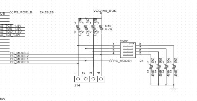
Figure 2.4.1 - Schematic diagram of PS_MODE circuit
| BOOT mode | Mode pin [3:0] | SW[4:1] |
| JTAG | 0000 | ON, ON, ON, ON |
| QSPI | 0010 | ON, ON, OFF, ON |
| SD | 0101 | ON, OFF, ON, OFF |
Table 2.4.1 - SW2 Startup Mode Configuration
2.5 DDR4 SDRAM
The board is equipped with eight Micron 1GB DDR4 chips, model MT40A512M16HA-083E. Four DDR4 chips are connected to the PS side, forming a 64-bit data bus bandwidth. Four DDR4 chips are connected to the PL side, also forming a 64-bit data bus bandwidth. The maximum operating speed of the PS-side DDR4 SDRAM is 2400Mb / s, and the four DDR4 memory systems are directly connected to the PS's BANK504 memory interface. The maximum operating data rate of the PL-side DDR SDRAM is 2400Mb / s, and the four DDR4 chips are connected to the FPGA's BANK64, 65, and 66 interfaces. The specific configuration of the PS-side and PL-side DDR4 SDRAM is shown in the table below:
| Location | Position | Chip Model | Capacity | Factory |
| PS | U39, U40, U41, U44 | MT40A512M16HA-083E | 512x16bit | Micron |
| PL | U51, U52, U54, U66 | MT40A512M16HA-083E | 512x16bit | Micron |
Table 2.5.1 - DDR4 Configuration
The hardware connection method for DDR4 on the PS side is shown in the following figure :
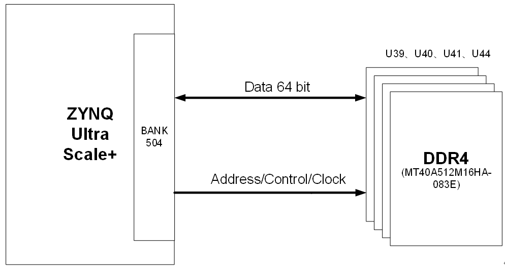
Figure 2.5.1 - Schematic diagram of DDR4 connection on the PS side
The hardware connection method of DDR4 on the P L side is shown in the figure below :
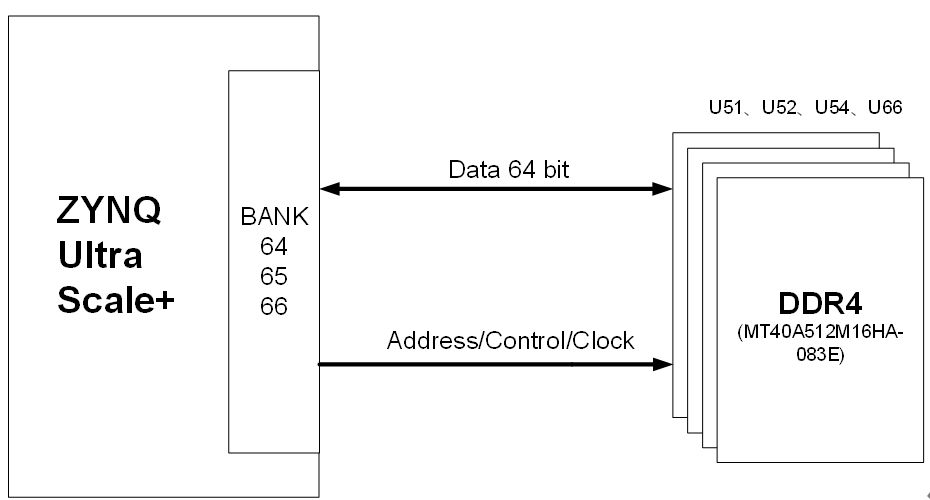
Figure 2.5.2 - Schematic diagram of DDR4 connection at the PL end
2.6 QSPI FLASH
The board is equipped with two MT25QU01GBBB8E12-0SIT serial Nor Flash memory chips in the PS, which can be used to store executable code and data, such as bootloaders, operating systems, and bitstreams. The two QSPI chips are connected in parallel.
To achieve higher performance, two Quad-SPI devices are connected in parallel, providing a total of 8 bits of data bus for booting and configuration . The interconnection method is shown below:
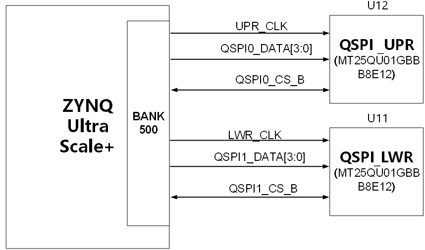
Figure 2.6.1 - Schematic diagram of interconnection between two QSPI Nor Flash chips and XCZU49DR
The pin definitions for the parallel connection of two QSPI Nor Flash chips are shown in the table below, and the pin definitions for the interconnection of the two QSPI Nor Flash chips are shown below:
| FPGA (U1) pin names | signal name | QSPI pin numbers | QSPI pin names |
| PS_MIO12_AV28 | MIO12_QSPI_UPR_CLK | U12.B2 | C |
| PS_MIO10_AV26 | MIO10_QSPI_UPR_DQ2 | U12.C4 | DQ2_W_B |
| PS_MIO9_AW26 | MIO9_QSPI_UPR_DQ1 | U12.D2 | DQ1 |
| PS_MIO8_AW27 | MIO8_QSPI_UPR_DQ0 | U12.D3 | DQ0 |
| PS_MIO11_AW28 | MIO11_QSPI_UPR_DQ3 | U12.D4 | DQ3_RST_HLD_B |
| PS_MIO7_AY27 | MIO7_QSPI_UPR_CS_B | U12.C2 | S_B |
| PS_MIO5_BA29 | MIO5_QSPI_LWR_CS_B | U11.C2 | S_B |
| PS_MIO4_BA28 | MIO4_QSPI_LWR_DQ0 | U11.D3 | DQ0 |
| PS_MIO3_BB28 | MIO3_QSPI_LWR_DQ3 | U11.D4 | DQ3_RST_HLD_B |
| PS_MIO2_BB26 | MIO2_QSPI_LWR_DQ2 | U11.C4 | DQ2_W_B |
| PS_MIO1_BA27 | MIO1_QSPI_LWR_DQ1 | U11.D2 | DQ1 |
| PS_MIO0_BB27 | MIO0_QSPI_LWR_CLK | U11.B2 | C |
Table 2.6.1 - Interconnect Pin Definitions for Two QSPI Nor Flash Chips
2.7 Micro SD Card Slot
The ZU49DR_COME includes a Micro SD card interface, providing user access to SD card storage for storing the boot program, Linux operating system kernel, file system, and other user data files. The SD card I/O signals are connected to the MIO signals of the PS BANK501. A schematic diagram of the PS and SD card connector connection is shown below:
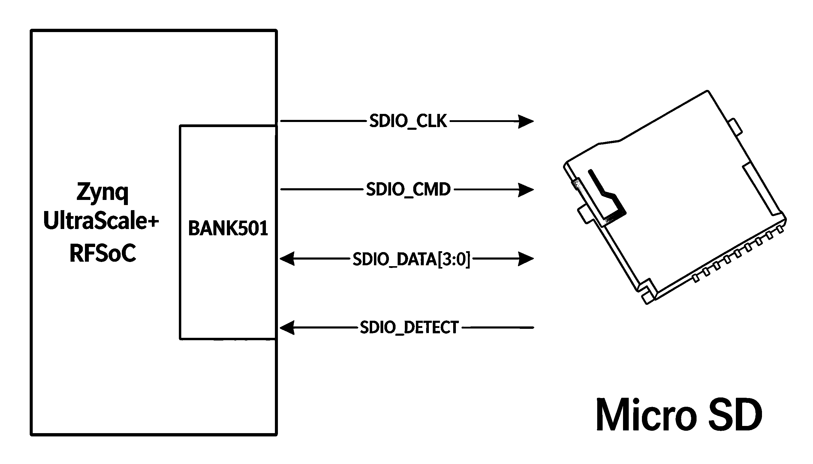
Figure 2.7.1 - SD Card Connection Diagram
| Signal name | pin name | pin number | Remark |
| MIO51_SDIO_CLK | PS_MIO51_M31 | M31 | SD clock signal |
| MIO50_SDIO_CMD | PS_MIO50_M30 | M30 | SD command signals |
| MIO46_SDIO_DAT0 | PS_MIO46_J31 | J31 | SD data Bit0 |
| MIO47_SDIO_DAT1 | PS_MIO47_L32 | L32 | SD data Bit1 |
| MIO48_SDIO_DAT2 | PS_MIO48_M32 | M32 | SD data Bit2 |
| MIO49_SDIO_DAT3 | PS_MIO49_K31 | K31 | SD data Bit3 |
| MIO45_SDIO_DETECT | PS_MIO45_L30 | L30 | SD card detection signal |
Table 2.7.1 - SD card pin assignments are as follows:
2.8 USB 3.0 interface
This board supports USB 3.0 on its PS side, supporting both HOST and SLAVE working modes, with a data transfer rate of up to 5.0Gb/s. The USB 3.0 port connects directly to an external Type-A interface, while the USB 2.0 port connects to an external USB3320C chip via the ULPI interface, enabling high-speed data communication between USB 3.0 and USB 2.0. A USB 3.0 connection diagram is shown below:
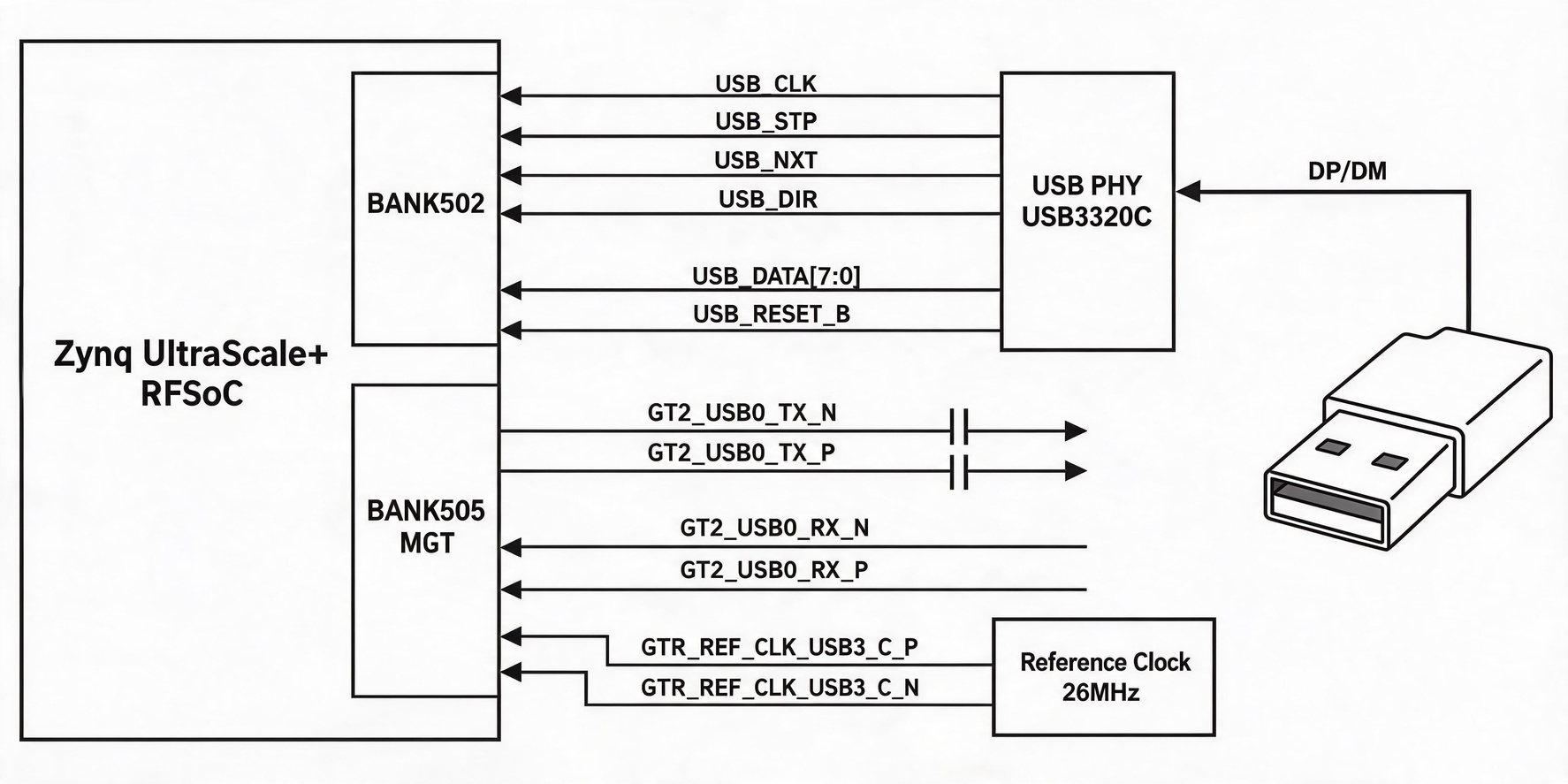
Figure 2.8.1 - Schematic diagram of USB 3.0 interface
| Signal name | pin name | ZYNQ pin number | Remark |
| MIO53_USB_DIR | PS_MIO53_N30 | N30 | USB 2.0 data direction signal |
| MIO52_USB_CLK | PS_MIO52_P28 | P28 | USB 2.0 clock signal |
| MIO63_USB_DATA7 | PS_MIO63_T29 | T29 | USB 2.0 data bit 7 |
| MIO62_USB_DATA6 | PS_MIO62_V28 | V28 | USB 2.0 data bit 6 |
| MIO61_USB_DATA5 | PS_MIO61_T28 | T28 | USB 2.0 data bit 5 |
| MIO60_USB_DATA4 | PS_MIO60_U28 | U28 | USB 2.0 data bit 4 |
| MIO59_USB_DATA3 | PS_MIO59_T30 | T30 | USB 2.0 data bit 3 |
| MIO58_USB_STP | PS_MIO58_R30 | R30 | USB 2.0 stop signal |
| MIO57_USB_DATA1 | PS_MIO57_R29 | R29 | USB 2.0 data bit 1 |
| MIO56_USB_DATA0 | PS_MIO56_N29 | N29 | USB 2.0 data bit 0 |
| MIO55_USB_NXT | PS_MIO55_P29 | P29 | USB 2.0 Next Data Signal |
| MIO54_USB_DATA2 | PS_MIO54_N28 | N28 | USB 2.0 data bit 2 |
| GT2_USB0_RX_N | PS_MGTRRXN2_505_AG42 | AG42 | USB 3.0 data transfer negative |
| GT2_USB0_RX_P | PS_MGTRRXP2_505_AG41 | AG41 | USB 3.0 data transfer is positive |
| GT2_USB0_TX_N | PS_MGTRTXN2_505_AF40 | AF40 | USB 3.0 data transmission negative |
| GT2_USB0_TX_P | PS_MGTRTXP2_505_AF39 | AF39 | USB 3.0 data transmission positive |
Table 2.8.1 - USB 3.0 Interface Pin Assignment
2.9 Ethernet
The ZU49DR_COME has three Gigabit Ethernet interfaces: one each on the PS and PL sides, with the third interface accessible via connector 3-1827253-6. The Ethernet chip used is the TI (Texas Instruments) DP83867IRRGZ, providing network communication services. The PS-side Ethernet PHY chip connects to the MIO port of the ZYNQ's PS-side BANK502, and the PL-side Ethernet PHY chip connects to the IO port of the ZYNQ's PL-side BANK67. The DP83867IRRGZ chip supports 10/100/1000 Mbps network transmission rates and communicates with the ZYNQ system's MAC layer via the RGMII interface. A schematic diagram of the Gigabit Ethernet PHY chip connection is shown below :
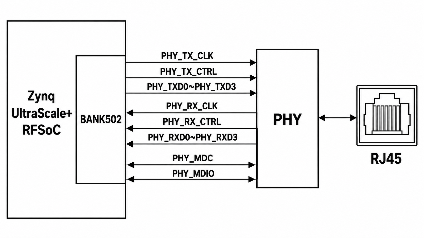
Figure 2.9.1 - Schematic diagram of Ethernet connection on PS end
| Signal name | pin name | pin number | PHY chip | |
| pin number | pin name | |||
| MIO64_ENET_TX_CLK | PS_MIO64_U30 | U30 | 29 | TX_CLK |
| MIO65_ENET_TX_D0 | PS_MIO65_V30 | V30 | 28 | TXD0 |
| MIO66_ENET_TX_D1 | PS_MIO66_V29 | V29 | 27 | TXD1 |
| MIO67_ENET_TX_D2 | PS_MIO67_W28 | W28 | 26 | TXD2 |
| MIO68_ENET_TX_D3 | PS_MIO68_Y29 | Y29 | 25 | TXD3 |
| MIO69_ENET_TX_CTRL | PS_MIO69_W29 | W29 | 37 | TX_CTRL |
| MIO70_ENET_RX_CLK | PS_MIO70_AA28 | AA28 | 32 | RXCLK |
| MIO71_ENET_RX_D0 | PS_MIO71_AB28 | AB28 | 33 | RXD0 |
| MIO72_ENET_RX_D1 | PS_MIO72_AC28 | AC28 | 34 | RXD1 |
| MIO73_ENET_RX_D2 | PS_MIO73_AA29 | AA29 | 35 | RXD2 |
| MIO74_ENET_RX_D3 | PS_MIO74_Y30 | Y30 | 36 | RXD3 |
| MIO75_ENET_RX_CTRL | PS_MIO75_AC29 | AC29 | 38 | RX_CTRL |
| MIO76_ENET_MDC | PS_MIO76_AB30 | AB30 | 16 | MDC |
| MIO77_ENET_MDIO | PS_MIO77_AA30 | AA30 | 17 | MDIO |
| ENET_RESET_B(MIO43_ETH_RESET#) | PS_MIO43_G31 | G31 | 43 | RESET_B |
Table 2.9.1 - PHY connection to XCZU49DR RFSoC PS terminal
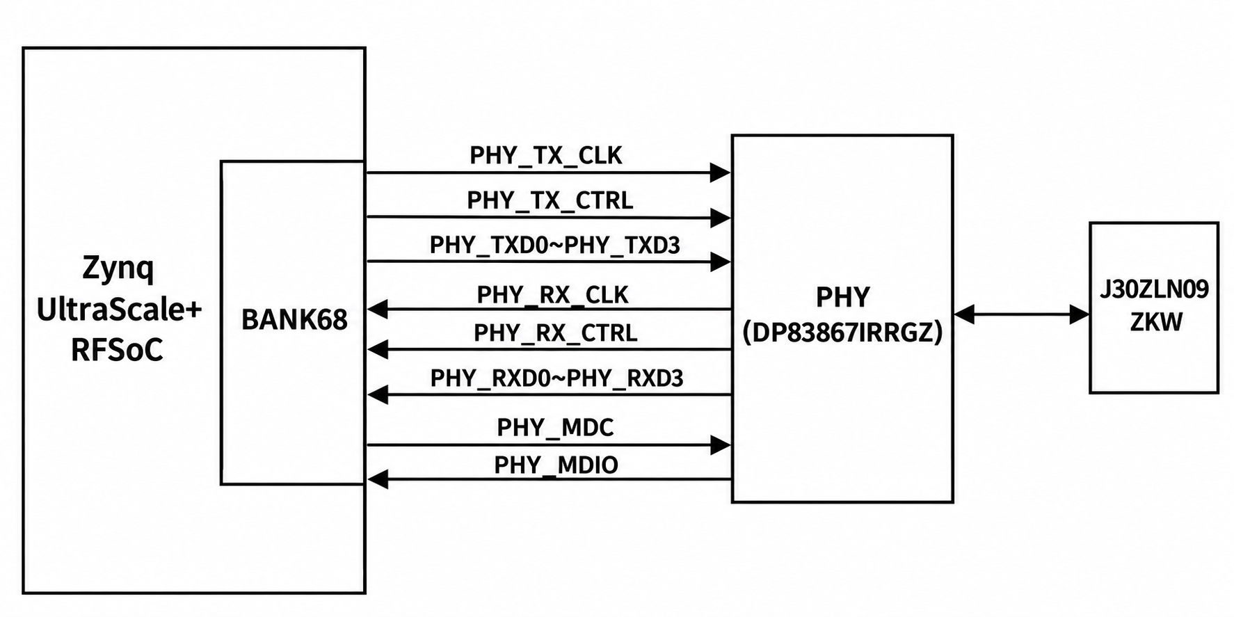
Figure 2.9.2 - Schematic diagram of Ethernet connection at the PL end
| Signal name | pin name | pin number | PHY chip | |
| pin number | pin name | |||
| PL_ENET_TX_CLK | IO_L14P_T2L_N2_GC_68_F23 | F23 | 29 | TX_CLK |
| PL_ENET_TX_D0 | IO_L18P_T2U_N10_AD2P_68_D23 | D23 | 28 | TXD0 |
| PL_ENET_TX_D1 | IO_L18N_T2U_N11_AD2N_68_C23 | C23 | 27 | TXD1 |
| PL_ENET_TX_D2 | IO_T2U_N12_68_E24 | E24 | 26 | TXD2 |
| PL_ENET_TX_D3 | IO_L19P_T3L_N0_DBC_AD9P_68_C26 | C26 | 25 | TXD3 |
| PL_ENET_TX_CTRL | IO_L19N_T3L_N1_DBC_AD9N_68_B26 | B26 | 37 | TX_CTRL |
| PL_ENET_RX_CLK | IO_L13P_T2L_N0_GC_QBC_68_H26 | H26 | 32 | RXCLK |
| PL_ENET_RX_D0 | IO_L15P_T2L_N4_AD11P_68_G25 | G25 | 33 | RXD0 |
| PL_ENET_RX_D1 | IO_L15N_T2L_N5_AD11N_68_F25 | F25 | 34 | RXD1 |
| PL_ENET_RX_D2 | IO_L16P_T2U_N6_QBC_AD3P_68_E22 | E22 | 35 | RXD2 |
| PL_ENET_RX_D3 | IO_L16N_T2U_N7_QBC_AD3N_68_D22 | D22 | 36 | RXD3 |
| PL_ENET_RX_CTRL | IO_L17P_T2U_N8_AD10P_68_E26 | E26 | 38 | RX_CTRL |
| PL_ENET_MDC | I O_L20N_T3L_N3_AD1N_68_C24 | C24 | 16 | MDC |
| PL_ENET_MDIO | IO_L21P_T3L_N4_AD8P_68_C25 | C25 | 17 | MDIO |
| PL_ETH_RESET# | IO_L2N_T1U_N11_GC_68_F22 | F22 | 43 | RESET_B |
Table 2.9.2 - PHY connection to XCZU49DR RFSoC PL terminal
2.10 Optical Port
The ZU49DR_COME has two QSFP interfaces. These two fiber optic interfaces connect to the GTY transceivers on the ZYNQ BANK129 and BANK130, respectively . CLK0 of the BANK129 and BANK130 are powered by differential crystal oscillators, with selectable clock frequencies of 156.25MHz or 106.25MHz. The CLK1 differential crystal oscillator on the BANK129 provides a 125MHz clock. A schematic diagram of the QSFP28 interface connection is shown below:
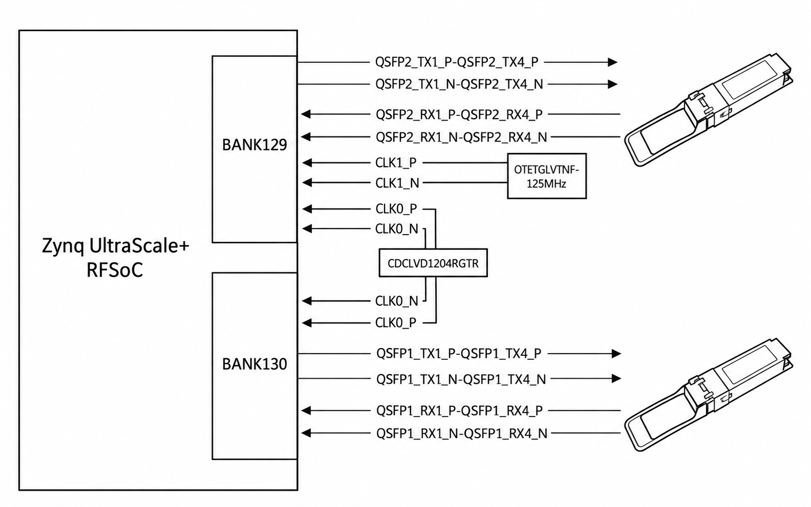
Figure 2.10.1 - Schematic diagram of fiber optic design
| Signal name | ZYNQ pin name | ZYNQ pin number |
| QSFP1_TX1_P | MGTYTXP0_130_K38 | K38 |
| QSFP1_TX1_N | MGTYTXN0_130_K39 | K39 |
| QSFP1_RX1_P | MGTYRXP0_130_L41 | L41 |
| QSFP1_RX1_N | MGTYRXN0_130_L42 | L42 |
| QSFP1_TX2_P | MGTYTXP1_130_J36 | J36 |
| QSFP1_TX2_N | MGTYTXN1_130_J37 | J37 |
| QSFP1_RX2_P | MGTYRXP1_130_J41 | J41 |
| QSFP1_RX2_N | MGTYRX N 1_130_J42 | J42 |
| QSFP1_TX3_P | MGTYTXP2_130_H38 | H38 |
| QSFP1_TX3_N | MGTYTXN2_130_H39 | H39 |
| QSFP1_RX3_P | MGTYRXP2_130_G41 | G41 |
| QSFP1_RX3_N | MGTYRX N 2_130_G42 | G42 |
| QSFP1_TX4_P | MGTYTXP3_130_G36 | G36 |
| QSFP1_TX4_N | MGTYTX N 3_130_G37 | G37 |
| QSFP1_RX4_P | MGTYRXP3_130_F39 | F39 |
| QSFP1_RX4_ N | MGTYRX N 3_130_F40 | F40 |
| QSFP2_TX1_P | MGTYTXP0_129_P38 | P38 |
| QSFP2_TX1_N | MGTYTXN0_129_P39 | P39 |
| QSFP2_RX1_P | MGTYRXP0_129_W41 | W41 |
| QSFP2_RX1_N | MGTYRXN0_129_W42 | W42 |
| QSFP2_TX2_P | MGTYTXP1_129_N36 | N36 |
| QSFP2_TX2_N | MGTYTXN1_129_N37 | N37 |
| QSFP2_RX2_P | MGTYRXP1_129_U41 | U41 |
| QSFP2_RX2_N | MGTYRXN1_129_U42 | U42 |
| QSFP2_TX3_P | MGTYTXP2_129_M38 | M38 |
| QSFP2_TX3_N | MGTYTXN2_129_M39 | M39 |
| QSFP2_RX3_P | MGTYRXP2_129_R41 | R41 |
| QSFP2_RX3_N | MGTYRXN2_129_R42 | R42 |
| QSFP2_TX4_P | MGTYTXP3_129_L36 | L36 |
| QSFP2_TX4_N | MGTYTXN3_129_L37 | L37 |
| QSFP2_RX4_P | MGTYRXP3_129_N41 | N41 |
| QSFP2_RX4_N | MGTYRXN3_129_N42 | N42 |
Table 2.10.1 - QSFP1 and QSFP2 Interface Pin Assignments
| Signal name | ZYNQ pin name | ZYNQ pin number | Remark |
| QSFP1_CLK_P | MGTREFCLK0P_130_P34 | P34 | The OUT0 output of the CDCLVD1204RGTR is configured at 156.25MHz by default, and can be set to 106.25MHz. |
| QSFP1_CLK_N | MGTREFCLK0N_130_P35 | P35 | The OUT0 output of the CDCLVD1204RGTR is configured at 156.25MHz by default, and can be set to 106.25MHz. |
| QSFP2_CLK_P | MGTREFCLK0P_129_V34 | V34 | The OUT1 output of the CDCLVD1204RGTR is configured at 156.25MHz by default, and can be set to 106.25MHz. |
| QSFP2_CLK_N | MGTREFCLK0N_129_V35 | V35 | The OUT1 output of the CDCLVD1204RGTR is configured at 156.25MHz by default, and can be set to 106.25MHz. |
| QSFP_REF_CLK_125M_P | MGTREFCLK1P_129_T34 | T34 | 125MHz differential output |
| QSFP_REF_CLK_125M_N | MGTREFCLK1N_129_T35 | T35 | 125MHz differential output |
Table 2.10.2 - Reference Clock Assignments for BANK129 and BANK130
Low-speed control I/O processing:
| QSFP low-speed IO signal name | Remark |
| MODSELL | pull down GND |
| ResetL | 3.3V pull-up |
| MODPRSL | 3.3V pull-up |
| SDA | 3.3V pull-up |
| SCL | 3.3V pull-up |
| intL | 3.3V pull-up |
| LPMode | 3.3V pull-up |
Table 2.10.3 - Fiber Optic Low-Speed I/O Signal Processing Methods:
2.11 NVMe
The ZU49DR_COME is equipped with a PCIe x4 standard M.2 interface for connecting NVMe SSDs. The M.2 interface uses an M-key slot and only supports PCI-E; users must select a PCIe type SSD. The PCIe signals are directly connected to the ZU49DR's BANK131 MGT transceiver. The four TX and RX signals are differentially connected to LANE0, LANE1, LANE2, and LANE3 of the MGT. The PCIe clock is provided by a 100MHz differential clock. The circuit design diagram is shown below:
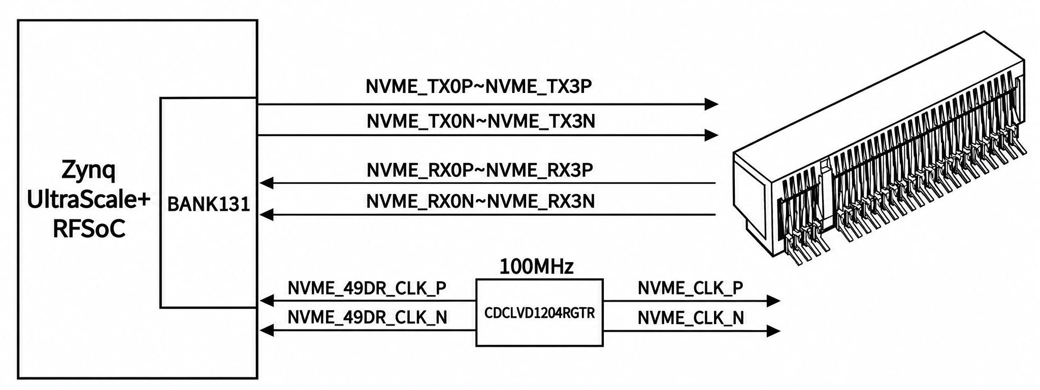
Figure 2.11.1 - M.2 Interface Design Schematic Diagram
| Signal name | ZYNQ pin name | NVMe connector U7 | |
| pin number | name | ||
| NVME_TX0P | MGTYTXP0_131_F34 | 49 | PERP0 |
| NVME_TX0N | MGTYTXP0_131_F35 | 47 | PERN0 |
| NVME_RX0P | MGTYRXP0_131_E41 | 43 | PETP0 |
| NVME_RX0N | MGTYRXP0_131_E42 | 41 | PETN0 |
| NVME_TX1P | MGTYRXP0_131_E36 | 37 | PERP1 |
| NVME_TX1N | MGTYRXP0_131_E37 | 35 | PERN1 |
| NVME_RX1P | MGTYRXP0_131_D39 | 31 | PETP1 |
| NVME_RX1N | MGTYRXP0_131_D40 | 29 | PETN1 |
| NVME_TX2P | MGTYRXP0_131_C36 | 25 | PERP2 |
| NVME_TX2N | MGTYRXP0_131_C37 | twenty three | PERN2 |
| NVME_RX2P | MGTYRXP0_131_C41 | 19 | PETP2 |
| NVME_RX2N | MGTYRXP0_131_C42 | 17 | PETN2 |
| NVME_TX3P | MGTYRXP0_131_A36 | 13 | PERP3 |
| NVME_TX3N | MGTYRXP0_131_A37 | 11 | PERN3 |
| NVME_RX3P | MGTYRXP0_131_B39 | 7 | PETP3 |
| NVME_RX3N | MGTYRXP0_131_B40 | 5 | PETN3 |
| NVME_49DR_CLK_P | MGTREFCLK0P_131_K34 | ||
| NVME_49DR_CLK_N | MGTREFCLK0N_131_K35 | ||
Table 2.11.1 - M.2 Interface ZYNQ Pin Assignment
2.12 Extension Interface
The ZU49DR_COME board has four additional I/O groups.
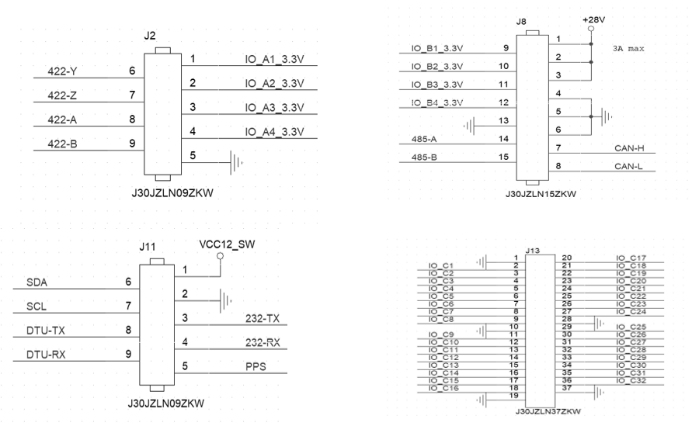
Figure 2.12.1 - Connection diagram of extended I/O circuit
| Signal name | ZYNQ pin name | ZYNQ pin number |
| IO_A1_3.3V | IO_L3P_AD13P_87_D14 | D14 |
| IO_A2_3.3V | IO_L2N_AD14N_87_D12 | D12 |
| IO_A3_3.3V | IO_L2P_AD14P_87_D13 | D13 |
| IO_A4_3.3V | IO_L1N_AD15N_87_E12 | E12 |
| 422-Y | IO_T2U_N12_69_E19 IO_L18N_T2U_N11_AD2N_69_D18 | |
| 422-Z | E19 | |
| 422-A | D18 | |
| 422-B |
Table 2.12.1 - J2 Extended I/O Pin Assignment
| Signal name | ZYNQ pin name | ZYNQ pin number | Remark |
| IO_B1_3.3V | IO_L3N_AD9N_89_H9 | H9 | |
| IO_B2_3.3V | IO_L3P_AD9P_89_H10 | H10 | |
| IO_B3_3.3V | IO_L2N_AD10N_89_J11 | J11 | |
| IO_B4_3.3V | IO_L2P_AD10P_89_J12 | J12 | |
| CAN-H | IO_L17P_T2U_N8_AD10P_69_E21 | E21 | CAN interface |
| CAN-L | IO_L16N_T2U_N7_QBC_AD3N_69_D17 | D17 | CAN interface |
| 485-A | IO_L21P_T3L_N4_AD8P_69_B21 | B21 | |
| 485-B | IO_L20P_T3L_N2_AD1P_69_C19 | C19 |
Table 2.12.2 - J8 Extended I/O Pin Assignment
| Signal name | ZYNQ pin name | ZYNQ pin number | Remark |
| SDA | PS_MIO15_AT27 | AT27 | I2C interface |
| SCL | PS_MIO14_AU27 | AU27 | I2C interface |
| DTU-TX | IO_L13N_T2L_N1_GC_QBC_69_G20 | G20 | |
| DTU-RX | IO_L13P_T2L_N0_GC_QBC_69_H20 | H20 | |
| 232-TX | IO_L15P_T2L_N4_AD11P_69_G21 | G21 | UART interface |
| 232-RX | IO_L14N_T2L_N3_GC_69_F18 | F18 | UART interface |
| PPS | IO_L18N_T2U_N11_AD2N_67_D27 | D27 |
Table 2.12.3 - J11 Extended I/O Pin Assignment
| Signal name | ZYNQ pin name | ZYNQ pin number |
| IO_C1 | IO_L12N_AD8N_87_F13 | F13 |
| IO_C2 | IO_L12P_AD8P_87_F14 | F14 |
| IO_C3 | IO_L6P_HDGC_87_F15 | F15 |
| IO_C4 | IO_L6N_HDGC_87_E14 | E14 |
| IO_C5 | IO_L9P_AD11P_87_E16 | E16 |
| IO_C6 | IO_L9N_AD11N_87_E15 | E15 |
| IO_C7 | IO_L10P_AD10P_87_D16 | D16 |
| IO_C8 | IO_L7P_HDGC_87_C15 | C15 |
| IO_C9 | IO_L10N_AD10N_87_C16 | C16 |
| IO_C10 | IO_L7N_HDGC_87_C14 | C14 |
| IO_C11 | IO_L8P_HDGC_87_B16 | B16 |
| IO_C12 | IO_L8N_HDGC_87_B15 | B15 |
| IO_C13 | IO_L11P_AD9P_87_A15 | A15 |
| IO_C14 | IO_L11N_AD9N_87_A14 | A14 |
| IO_C15 | IO_L5P_HDGC_87_A13 | A13 |
| IO_C16 | IO_L5N_HDGC_87_A12 | A12 |
| IO_C17 | IO_L5P_HDGC_AD7P_89_G12 | G12 |
| IO_C18 | IO_L5N_HDGC_AD7N_89_G11 | G11 |
| IO_C19 | IO_L6N_HDGC_AD6N_89_F9 | F9 |
| IO_C20 | IO_L6P_HDGC_AD6P_89_F10 | F10 |
| IO_C21 | IO_L7N_HDGC_AD5N_89_E9 | E9 |
| IO_C22 | IO_L9P_AD3P_89_D9 | D9 |
| IO_C23 | IO_L7P_HDGC_AD5P_89_E10 | E10 |
| IO_C24 | IO_L8P_HDGC_AD4P_89_E11 | E11 |
| IO_C25 | IO_L12N_AD0N_89_A9 | A9 |
| IO_C26 | IO_L9N_AD3N_89_C9 | C9 |
| IO_C27 | IO_L12P_AD0P_89_A10 | A10 |
| IO_C28 | IO_L11N_AD1N_89_B10 | B10 |
| IO_C29 | IO_L10N_AD2N_89_B11 | B11 |
| IO_C30 | IO_L8N_HDGC_AD4N_89_D11 | D11 |
| IO_C31 | IO_L10P_AD2P_89_C11 | C11 |
| IO_C32 | IO_L11P_AD1P_89_C10 | C10 |
Table 2.12.4 - J13 Extended I/O Pin Assignment
2.13 RF
The product supports 16 channels of 14-bit ADC 2.5GSPS input and 16 channels of 14-bit DAC 9.85 GSPS output. The RF connector is 190-0108-AAD1, with single-ended signal input and output. Differential to single-ended conversion is performed through a balun device to complete data transmission and reception. The VCM signal is also brought out to the TP for easy adjustment of the common-mode voltage.
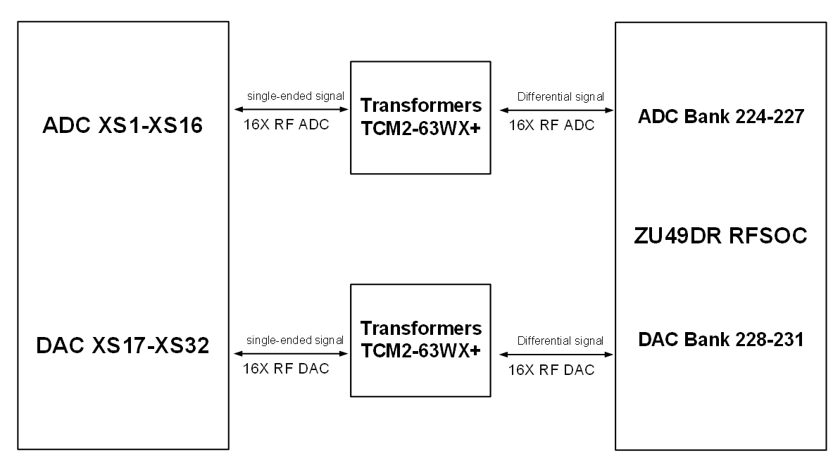
Figure 2.13.1 - ADC & DAC Connection Diagram
| Signal name | ZYNQ pin name | ZYNQ pin number |
| ADC224_T0_CH0_P | ADC_VIN0_P_224_AU5 | AU5 |
| ADC224_T0_CH0_N | ADC_VIN0_N_224_AU4 | AU4 |
| ADC224_T0_CH1_P | ADC_VIN1_P_224_AU2 | AU2 |
| ADC224_T0_CH1_N | ADC_VIN1_N_224_AU1 | AU1 |
| ADC224_T0_CH2_P | ADC_VIN2_P_224_AR5 | AR5 |
| ADC224_T0_CH2_N | ADC_VIN2_N_224_AR4 | AR4 |
| ADC224_T0_CH3_P | ADC_VIN3_P_224_AR2 | AR2 |
| ADC224_T0_CH3_N | ADC_VIN3_N_224_AR1 | AR1 |
| ADC225_T1_CH0_P | ADC_VIN0_P_225_AN5 | AN5 |
| ADC225_T1_CH0_N | ADC_VIN0_N_225_AN4 | AN4 |
| ADC225_T1_CH1_P | ADC_VIN1_P_225_AN2 | AN2 |
| ADC225_T1_CH1_N | ADC_VIN1_N_225_AN1 | AN1 |
| ADC225_T1_CH2_P | ADC_VIN2_P_225_AL5 | AL5 |
| ADC225_T1_CH2_N | ADC_VIN2_N_225_AL4 | AL4 |
| ADC225_T1_CH3_P | ADC_VIN3_P_225_AL2 | AL2 |
| ADC225_T1_CH3_N | ADC_VIN3_N_225_AL1 | AL1 |
| ADC226_T2_CH0_P | ADC_VIN0_P_226_AJ5 | AJ5 |
| ADC226_T2_CH0_N | ADC_VIN0_N_226_AJ4 | AJ4 |
| ADC226_T2_CH1_P | ADC_VIN1_P_226_AJ2 | AJ2 |
| ADC226_T2_CH1_N | ADC_VIN1_N_226_AJ1 | AJ1 |
| ADC226_T2_CH2_P | ADC_VIN2_P_226_AG5 | AG5 |
| ADC226_T2_CH2_N | ADC_VIN2_N_226_AG4 | AG4 |
| ADC226_T2_CH3_P | ADC_VIN3_P_226_AG2 | AG2 |
| ADC226_T2_CH3_N | ADC_VIN3_N_226_AG1 | AG1 |
| ADC227_T3_CH0_P | ADC_VIN0_P_227_AE5 | AE5 |
| ADC227_T3_CH0_N | ADC_VIN0_N_227_AE4 | AE4 |
| ADC227_T3_CH1_P | ADC_VIN1_P_227_AE2 | AE2 |
| ADC227_T3_CH1_N | ADC_VIN1_N_227_AE1 | AE1 |
| ADC227_T3_CH2_P | ADC_VIN2_P_227_AC5 | AC5 |
| ADC227_T3_CH2_N | ADC_VIN2_N_227_AC4 | AC4 |
| ADC227_T3_CH3_P | ADC_VIN3_P_227_AC2 | AC2 |
| ADC227_T3_CH3_N | ADC_VIN3_N_227_AC1 | AC1 |
| DAC228_T0_CH0_P | DAC_VOUT0_P_228_Y5 | Y5 |
| DAC228_T0_CH0_N | DAC_VOUT0_N_228_Y4 | Y4 |
| DAC228_T0_CH1_P | DAC_VOUT1_P_228_Y2 | Y2 |
| DAC228_T0_CH1_N | DAC_VOUT1_N_228_Y1 | Y1 |
| DAC228_T0_CH2_P | DAC_VOUT2_P_228_V5 | V5 |
| DAC228_T0_CH2_N | DAC_VOUT2_N_228_V4 | V4 |
| DAC228_T0_CH3_P | DAC_VOUT3_P_228_V2 | V2 |
| DAC228_T0_CH3_N | DAC_VOUT3_N_228_V1 | V1 |
| DAC229_T1_CH0_P | DAC_VOUT0_P_229_T5 | T5 |
| DAC229_T1_CH0_N | DAC_VOUT0_N_229_T4 | T4 |
| DAC229_T1_CH1_P | DAC_VOUT1_P_229_T2 | T2 |
| DAC229_T1_CH1_N | DAC_VOUT1_N_229_ T1 | T1 |
| DAC229_T1_CH2_P | DAC_VOUT2_P_229_P5 | P5 |
| DAC229_T1_CH2_N | DAC_VOUT2_N_229_P4 | P4 |
| DAC229_T1_CH3_P | DAC_VOUT3_P_229_P2 | P2 |
| DAC229_T1_CH3_N | DAC_VOUT3_N_229_P1 | P1 |
| DAC230_T2_CH0_P | DAC_VOUT0_P_230_M5 | M5 |
| DAC230_T2_CH0_N | DAC_VOUT0_N_230_M4 | M4 |
| DAC230_T2_CH1_P | DAC_VOUT1_P_230_M2 | M2 |
| DAC230_T2_CH1_N | DAC_VOUT1_N_230_M1 | M1 |
| DAC230_T2_CH2_P | DAC_VOUT2_P_230_K5 | K5 |
| DAC230_T2_CH2_N | DAC_VOUT2_N_230_K4 | K4 |
| DAC230_T2_CH3_P | DAC_VOUT3_P_230_K2 | K2 |
| DAC230_T2_CH3_N | DAC_VOUT3_N_230_K1 | K1 |
| DAC231_T3_CH0_P | DAC_VOUT0_P_231_H5 | H5 |
| DAC231_T3_CH0_N | DAC_VOUT0_N_231_H4 | H4 |
| DAC231_T3_CH1_P | DAC_VOUT1_P_231_H2 | H2 |
| DAC231_T3_CH1_N | DAC_VOUT1_N_231_H1 | H1 |
| DAC231_T3_CH2_P | DAC_VOUT2_P_231_F5 | F5 |
| DAC231_T3_CH2_N | DAC_VOUT2_N_231_F4 | F4 |
| DAC231_T3_CH3_P | DAC_VOUT3_P_231_F2 | F2 |
| DAC231_T3_CH3_N | DAC_VOUT3_N_231_F1 | F1 |
Table 2.13.1 - ADC and DAC Pin Assignment Table
2.14 COME
Figure 2.14.1 - Schematic diagram of USB 3.0 at the COME end
| Signal name | U21 pin name | U21 pin number |
| USB_SSRX0_- | USB_SSRX0- | A22 |
| USB_SSRX0_+ | USB_SSRX0+ | A23 |
| USB_SSTX0_- | USB_SSTX0- | B22 |
| USB_SSTX0_+ | USB_SSTX0+ | B23 |
| USB0_- | USB0_- | A45 |
| USB0_+ | USB0_+ | A46 |
| USB_SSRX1_- | USB_SSRX1- | A25 |
| USB_SSRX1_+ | USB_SSRX1+ | A26 |
| USB_SSTX1_- | USB_SSTX1- | B25 |
| USB_SSTX1_+ | USB_SSTX1+ | B26 |
| USB1_- | USB1_- | B45 |
| USB1_+ | USB1_+ | B46 |
Table 2.14.1 - Pin Correspondence of USB 3.0 Pins on the COME Side
- Ethernet : The COME port of the board supports Ethernet communication for data transmission, and is brought out through HR911130CE.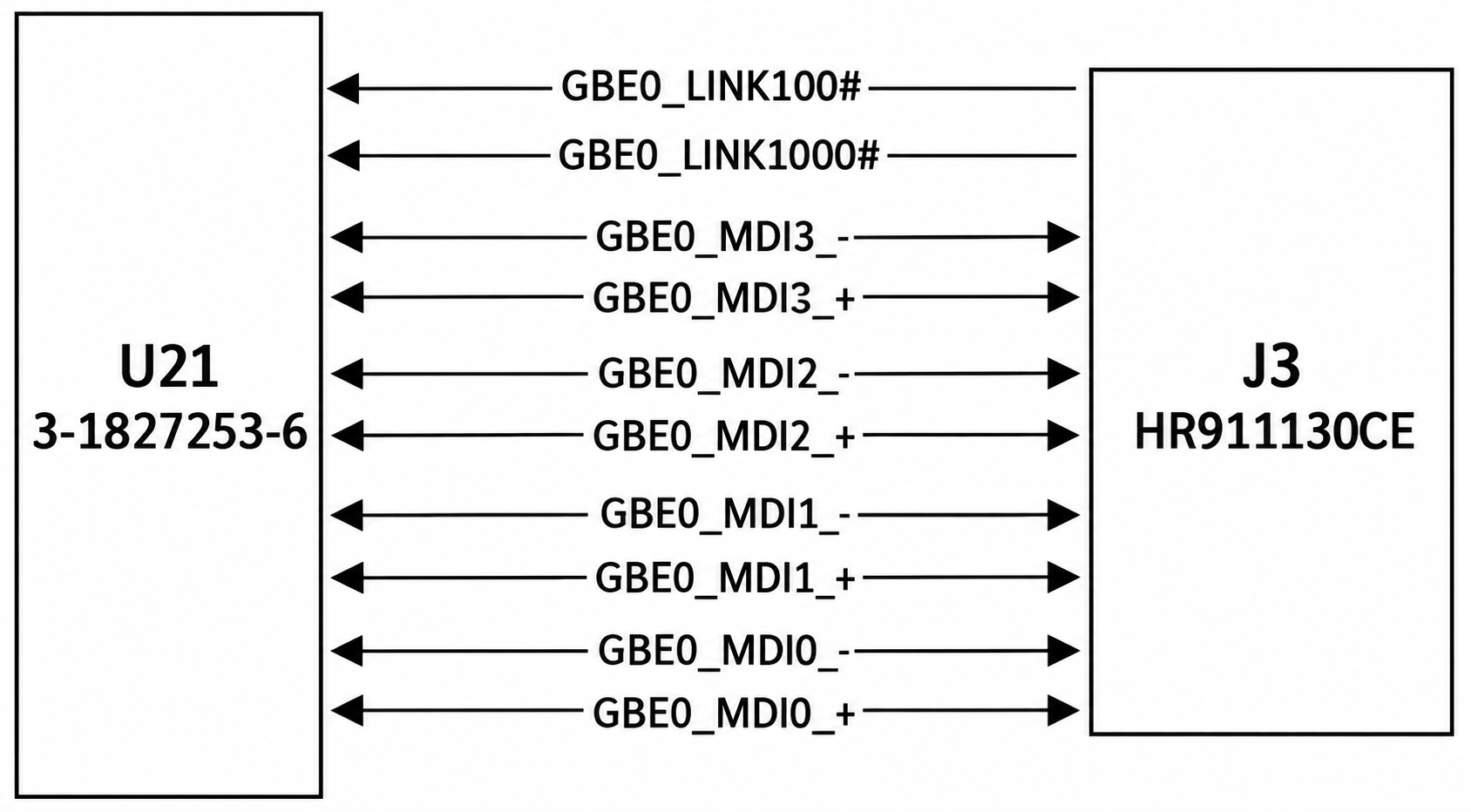
Figure 2.14.2 - Schematic diagram of Ethernet at the COME end
| Signal name | U21 pin name | U21 pin number |
| GBE0_LINK100# | GBE0_LINK100# | A4 |
| GBE0_LINK1000# | GBE0_LINK1000# | A5 |
| GBE0_MDI0_- | GBE0_MDI0- | A12 |
| GBE0_MDI0_+ | GBE0_MDI0+ | A13 |
| GBE0_MDI1_- | GBE0_MDI1- | A9 |
| GBE0_MDI1_+ | GBE0_MDI1+ | A10 |
| GBE0_MDI2_- | GBE0_MDI2- | A6 |
| GBE0_MDI2_+ | GBE0_MDI2+ | A7 |
| GBE0_MDI3_- | GBE0_MDI3- | A2 |
| GBE0_MDI3_+ | GBE0_MDI3+ | A3 |
Table 2.14.2 - Ethernet Pin Correspondence Table for COME Terminal
- Display Port : COME side DisplayPort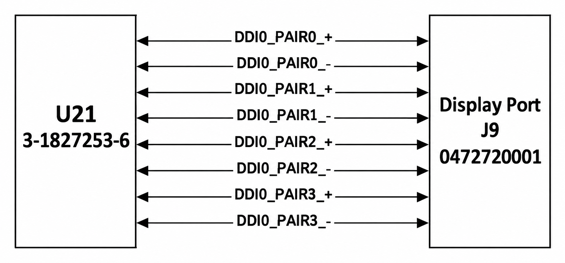
Figure 2.14.3 - Schematic diagram of COME-side Display Port
| Signal name | U21 pin name | U21 pin number |
| DDI0_PAIR0_+ | DDI0_PAIR0+/SDVO1_RED+ | B71 |
| DDI0_PAIR0_- | DDI0_PAIR0-/SDVO1_RED | B72 |
| DDI0_PAIR1_+ | DDI0_PAIR1+/SDVO1_GRN+ | B73 |
| DDI0_PAIR1_- | DDI0_PAIR1-/SDVO1_GRN | B74 |
| DDI0_PAIR2_+ | DDI0_PAIR2+/SDVO1_BLU+ | B75 |
| DDI0_PAIR2_- | DDI0_PAIR2-/SDVO1_BLU | B76 |
| DDI0_PAIR3_+ | DDI0_PAIR3+/SDVO1_CK+ | B81 |
| DDI0_PAIR3_- | DDI0_PAIR3-/SDVO1_CK | B82 |
| DDI0_CTRLCLK_AUX_+ | DDI0_CTRLCLK_AUX_+ | B98 |
| DDI0_CTRLDAT_AUX_- | DDI0_CTRLDAT_AUX_- | B99 |
| DDI0_HPD | DDI0_HPD | B89 |
| DDI0_DDC_AUX_SEL | DDI0_DDC_AUX_SEL | B95 |
Table 2.14.3 - COME Display Port Pin Correspondence Table
- Storage : The AXD embedded storage chip is extended on the board via the COME terminal, achieving extremely low write power consumption and extending SSD lifespan. It also provides extremely high IOPS performance, high reliability, and can operate in a wide temperature range. This provides an onboard storage solution for embedded boards, fully leveraging the ultra-high performance and low power consumption characteristics of Gen4 to offer ample storage capacity and read/write speeds. It is widely applicable to server, automotive, and shipboard applications.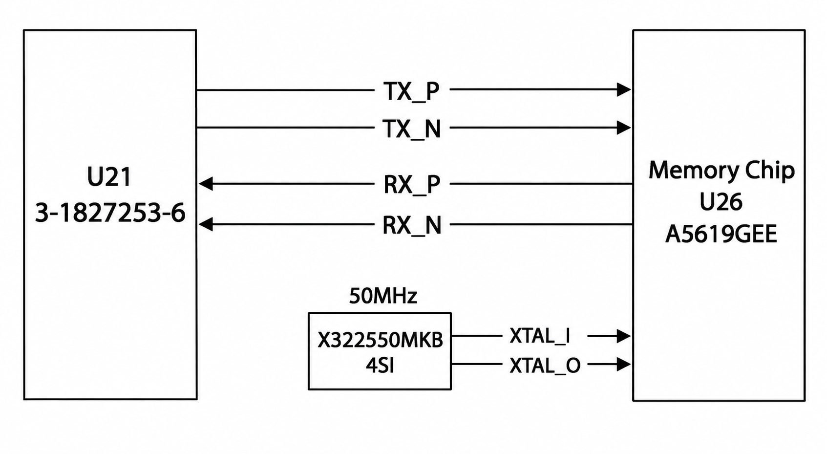
Figure 2.14.4 - Schematic diagram of COME-side storage
| Signal name | U21 pin name | U21 pin number |
| RX_P | SATA0_TX+ | A16 |
| RX_N | SATA0_TX- | A17 |
| TX_P | SATA0_RX+ | A19 |
| TX_N | SATA0_RX- | A20 |
Table 2.14.4 - COME Side Storage Pin Assignment Table
2.15 Clock Configuration
The Zynq UltraScale RFSoC offers multiple clock options, with dual crystal oscillators on the core module. The system clock defaults to a 33.33MHz active crystal oscillator. The X1 crystal operates at 32.768kHz, driving the internal RTC circuitry. A schematic diagram of the clock circuit design is shown below:
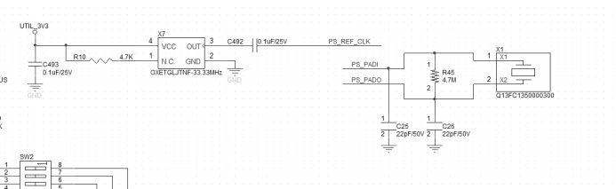
Figure 2.15.1 - Crystal oscillator schematic diagram
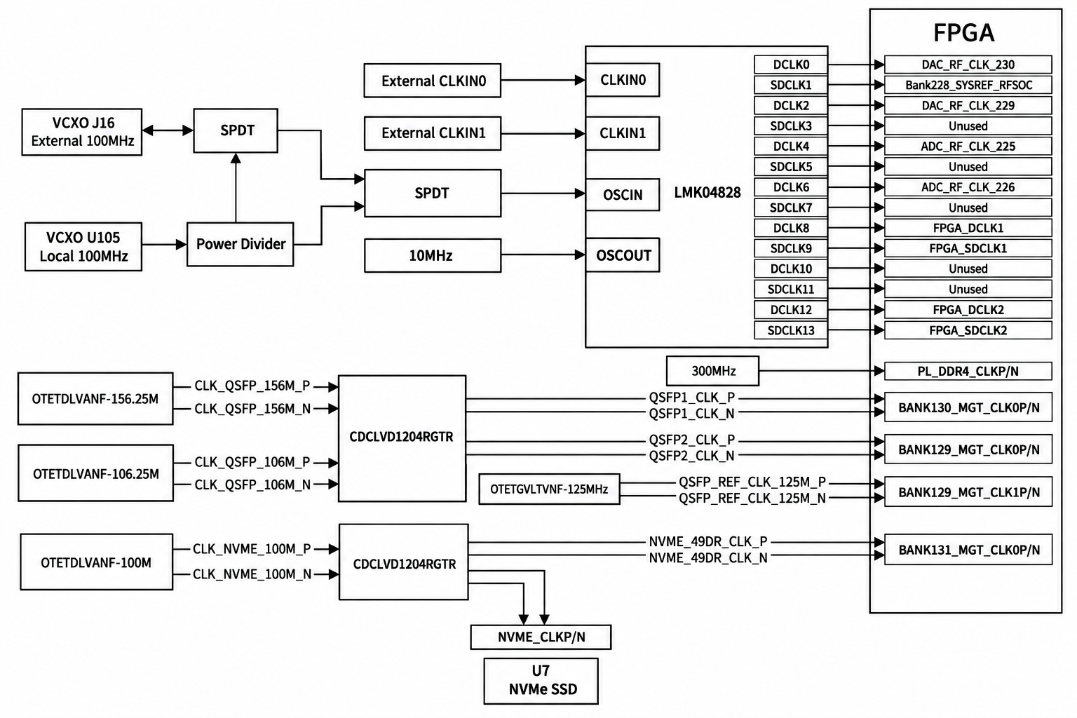
Figure 2.15.2 - Clock Distribution Connection Diagram
The system uses the LMK04828 clock chip to distribute the clock signals required by the ADC and DAC. The LMK04828's CLKIN0 and CLKIN1 are external differential inputs. OSCIN provides two input methods: one using a 100MHz high-stability OCXO, and the other an external input clock. The board also supports one external output clock (100MHz). The external output clock and the external input clock share a single J16 SMP channel. The external input and board output clock channels cannot be used simultaneously; only one scenario can be selected at a time.
Note: When using OSCIN as an external clock source, the power supply enable of the local clock needs to be disabled to prevent interference between the two clocks.
- Scenario 1 : The input source is a local OCXO, which can also output one 100MHz clock signal. The OCXO's power supply needs to be enabled .
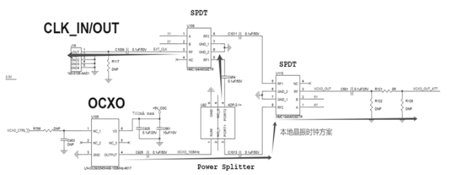
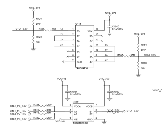
Figure 2.15.1 - Scenario 1: Circuit diagram of input source using local OCXO 100MHz
- Scenario 2 : An external clock is selected as the input source, and the power supply enable of the OCXO needs to be disabled.
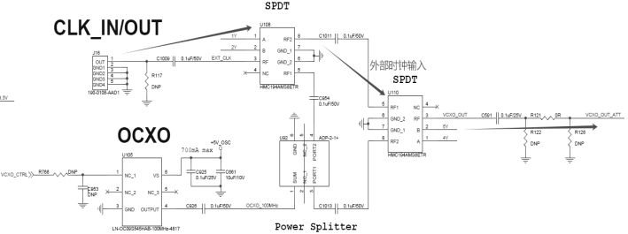
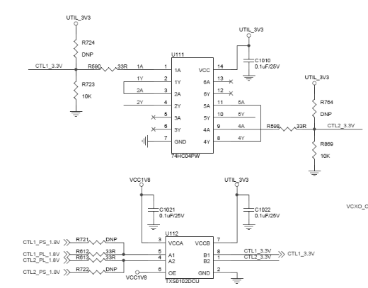
Figure 2.15.2 - Scenario 2: Circuit diagram of input source using external clock.
The control logic for the two scenarios above is as follows:
| Scene 1 | Scene 2 | |||
| pin | CTL2_PL_1.8V | CTL1_PL_1.8V | CTL1_PL_1.8V | CTL2_PL_1.8V |
| constraint | BB9 | AY9 | AY9 | BB9 |
| Level | Low | high | Low | high |
| Local crystal oscillator | pin | +5V_OSC_EN | pin | +5V_OSC_EN |
| constraint | H30 | constraint | H30 | |
| Level | high | Level | Low | |
Table 2.15.1 - Control Logic:
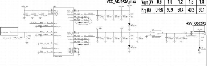
Figure 2.15.3 - Location markings for OCXO power supply +5V_OSC and +5V_OSC_EN
2.16 Power Supply
The ZU49DR_COME uses a DC 24V~32V power input and outputs 12V power through an LTM4613. The 12V system power supply is converted into different voltages by a buck regulator to drive the FPGA and other circuits on the board. The power supply for the board's ADC and DAC is provided by a linear low-voltage LDO, which has good power supply rejection (PSRR).
The ZU49DR_COME power supply design block diagram is shown below:
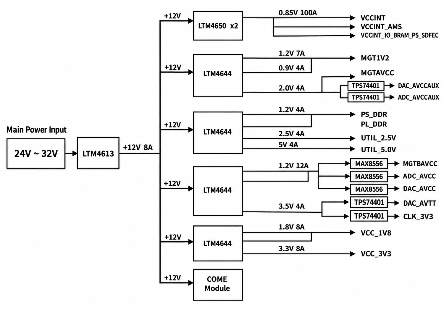
Figure 2.16.1 - ZU49DR_COME Power Supply Design Block Diagram
| BANK | Level (V) | Remark |
| BANK67, 68, 69 | 1.8V | HP BANK |
| BANK84, 88 | 1.8V | HD BANK |
| BANK87, 89 | 3.3V | HD BANK |
| BANK 128, 129, 130, 131 | 1.2V | QSFP (BANK129, 130), PCIE (BANK128), NVME (BANK131) |
| BANK500, 501, 502 | 1.8V | MIO |
| BANK503 | 1.8V fixed | Configure pin outputs, mode selection, and system reset signal. |
Table 2.16.1 - IO BANK Interface Levels of ZU49DR_COME
2.17 Structural diagram
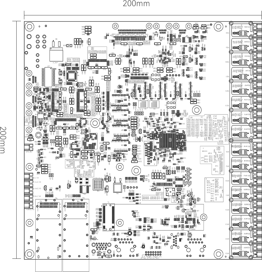
Figure 2.17.1 - Front view of ZU49DR_COME structure
Appendix: List of Abbreviations
| Abbreviation | Full English Name | Description |
| PS | Processor System | Processor System |
| PL | Programmable Logic | Programmable Logic |
| SOC | System on Chip | System on Chip |
| DDR3 | Double Data Rate 3 SDRAM | Double Data Rate 3 SDRAM |
| eMMC | Embedded Multi Media Card | Embedded MultiMediaCard |
| QSPI | Quad Serial Peripheral Interface | Quad Serial Peripheral Interface |
| GTP | Gigabit Transceiver | Gigabit Transceiver |
| UART | Universal Asynchronous Receiver/Transmitter | Universal Asynchronous Receiver/Transmitter |
| HDMI | High-Definition Multimedia Interface | High-Definition Multimedia Interface |
| PCIe | Peripheral Component Interconnect Express | Peripheral Component Interconnect Express |
| USB | Universal Serial Bus | Universal Serial Bus |
| JTAG | Joint Test Action Group | Joint Test Action Group |
| SFP | Small Form-factor Pluggable | Small Form-factor Pluggable |
| MIO | Multiplexed I/O | Multiplexed I/O |
| GPHY | Gigabit Ethernet PHY | Gigabit Ethernet PHY |
| I2C | Inter-Integrated Circuit | Inter-Integrated Circuit |
| RGMII | Reduced Gigabit Media Independent Interface | Reduced Gigabit Media Independent Interface |
| RMII | Reduced Media Independent Interface | Reduced Media Independent Interface |
| LED | Light Emitting Diode | Light Emitting Diode |
| LVDS | Low-Voltage Differential Signaling | Low-Voltage Differential Signaling |
Contact information
Alinx Electronic Limited
Company Website: www.en.alinx.com
Service Hotline:+86 21 67676997
Technical Support:technical@alinx.com