
Appearance
AXW47 User Manual

Alinx Electronic Limited
Company Website: www.en.alinx.com
Service Hotline:+86 21 67676997
Technical Support : technical@alinx.com
Document Information
| Item | Content |
| Document Name | Product Manual |
| Product Model | AXW47 |
| Document Version | V1.0 |
| Prepared by | Alinx Electronic Limited |
| Release Date | 2026.9.28 |
Document Revision History
| Version | Date | Section | Revision Summary |
| V1.0 | 2026.9.28 | All | Initial Release |
Part 1:Development Board Introduction
The development board consists of a SoM and a carrier board, which are connected by a high-speed inter-board connector.
The SoM utilizes the Xilinx Zynq™ UltraScale+™ RFSoC Gen3 series ZU47DR FPGA main chip, which supports 8-channel 14-bit RF-ADCs with a maximum sampling rate of 5 GSPS and 8-channel 14-bit RF-DACs with a maximum sampling rate of 9.85 GSPS. This reduces the complexity of the RF signal processing chain, maximizes input/output channel density without sacrificing bandwidth, leverages heterogeneous processing capabilities, and offers lower power consumption (eliminating ADC/DAC components and reducing FPGA-to-analog interface power consumption). The Zynq UltraScale+ device provides an ARM Cortex-A53 processing subsystem, UltraScale+ programmable logic, and the highest signal processing bandwidth, enabling a comprehensive RF signal chain to meet the needs of wireless, cable TV access, test and measurement, early warning/radar, and other high-performance RF applications.
The carrier board expands the SoM with a rich array of peripheral interfaces and includes a pure logic KU115 FPGA chip to provide broader back-end data processing capabilities. These include one SD card interface, two USB 3.0 interfaces, one Gigabit Ethernet interface, two JTAG/UART interfaces, one SFP interface, two QSFP interfaces, four NVMe interfaces, and two MGB interfaces (expandable to PCIe). The image below shows the actual physical prototype of the entire development system.
The RFSoC and KU115 are interconnected via 8 sets of high-speed GTs, with a throughput of 80Gbps, which increases the data processing capability of the RFSoC.
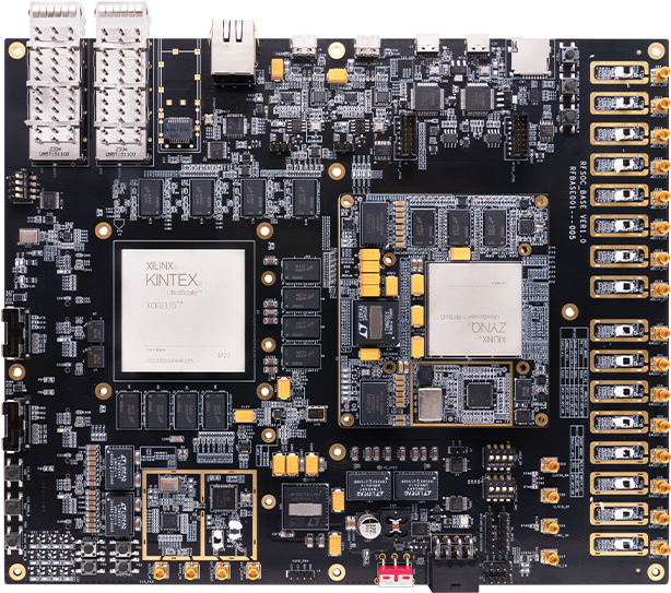
Figure 1.1.1 - Physical image of the development board
This physical image shows the interfaces and functions that the development platform can include.
The SoM consists of ZU47DR + 4GB DDR4 (PS) + 2GB DDR4 (PL) + 1Gb QSPI Flash + 32GBeMMC . In addition, the core module provides dual crystal clock sources: a single-ended 33.3333MHz active crystal oscillator for the PS system and a 32.768kHz crystal to drive the RFSoC internal RTC circuit.
M.2 Interface : A 4-way PCIe x 4 standard M.2 interface for connecting M.2 SSD solid-state drives.
USB 3.0 ports : 2 USB 3.0 ports, supporting both HOST and SLAVE modes.
Gigabit Ethernet interface : One 10M/100M/1000M Ethernet RJ45 interface for Ethernet data exchange with computers or other network devices.
JTAG & UART Interface : The two-channel JTAG & UART debug interface is a Type-C interface. JTAG and UART share this interface and are used for downloading and debugging FPGA programs.
Micro SD Card Slot : One Micro SD card slot for storing operating system images and file systems.
QSFP fiber optic interfaces : 2 QSFP fiber optic interfaces, supporting a communication rate of 40G.
SFP Fiber Optic Interface : One SFP interface, supporting 10G communication speed.
Expandable MGB interface : 2 MGB interfaces, expandable to 2 PCIe x4.
Storage : The carrier board is expanded with four 4GB DDR4 modules and one 1Gb QSPI Flash module .
Extended I/O : 2 sets of extended I/O, 1 set of PL-side extended I/O, and 1 set of PS-side extended I/O, which can be customized by the user.
LED lights : 4 expandable LED lights on the RFSoC side and 8 expandable LED lights on the KU115 side, for user customization.
Buttons : The RFSoC side has 5 additional buttons , and the KU115 side has 2 additional reset buttons and a four-position DIP switch, which can be customized by the user .
Part 2:SoM Introduction
The 47DR SoM is based on the Zynq UltraScale+ RFSoC series XCZU47DR-FFVE1156 (hereinafter referred to as XCZU47DR). This series integrates key subsystems of multi-band, multi-mode cellular radio and cable infrastructure (DOCSIS) into a single SoC platform, which includes a feature-rich 64-bit quad-core Arm® Cortex-A53 and dual-core Arm Cortex-R5F processing system.
The main chip, XCZU47DR, supports 8-channel 14-bit RF-ADC with a maximum sampling rate of 5 GSPS and 8-channel 14-bit RF-DAC with a maximum sampling rate of 9.85 GSPS. This reduces the complexity of the RF signal processing chain, maximizes input/output channel density without sacrificing bandwidth, utilizes heterogeneous processing capabilities, and boasts lower power consumption (eliminating ADC/DAC components and reducing FPGA-to-analog interface power consumption). Zynq UltraScale+ devices offer an ARM Cortex-A53 processing subsystem, UltraScale+ programmable logic, and the highest signal processing bandwidth, providing a comprehensive RF signal chain to meet the needs of wireless, cable TV access, test and measurement, early warning/radar, and other high-performance RF applications.
2.1 Product Overview
The 47DR SoM incorporates the AMD RFSoC in its most versatile design, enabling use across a wide range of scenarios. The SoM receives 12V power from the carrier board through boardtoboard connectors. The 47DR SoM uses six Micron DDR4 chips, model MT40A512M16LY062E IT:E. Four DDR4 chips are mounted on the PS side to form a 64bit data bus width, while two DDR4 chips are mounted on the PL side to form a 32bit data bus width. Each DDR4 chip has a capacity of 1GB. The DDR4 SDRAM supports data rates up to 3200 MT/s, and a 32GB eMMC is also provided. In addition, two 1Gbit NOR FLASH devices are integrated on the module for boot storage, configuration, and system files.
To interface with the carrier board, the module uses three 240pin boardtoboard connectors to expand: 2 HD Banks, 2 PS MIO Banks, 8× PL GTY (up to 28.21 Gb/s), 4× PS GTR (up to 6 Gb/s), 13 IOs (HP Bank), 8 highspeed RF ADCs, 8 highspeed DACs, and JTAG.
2.2 Application Scenarios
2.3 Product Features
The XCZU47DR FPGA chip integrates an RF direct sampling data converter, FPGA logic, a complete ARM processor subsystem, and a high-speed transceiver.
It supports 8 channels of 14-bit RF-ADC and 8 channels of 14-bit RF-DAC, providing a comprehensive RF signal chain to maximize input/output channel density, high bandwidth, heterogeneous processing capabilities, and low power consumption.
The product can meet the needs of different application scenarios, as well as the needs of high-performance RF applications.
Abundant information and resources: We provide complete board information and design resources, offer suggestions for secondary development, and continuously collect customer feedback to improve our support.
Collaborating with open-source projects: The board is among the first to partner with the MAGI Project, providing a wealth of flexible and configurable IPs to shorten customers' design and verification cycles.
Low cost and high cost performance: It has a lower price and more features compared to similar products.
High integration: leveraging MPSoC Its advantage lies in its ability to perform complex and heterogeneous tasks on-chip, which can significantly reduce debugging and development cycles compared to traditional multi-chip heterogeneous designs.
2.4 Appearance
The image below shows the appearance of the 47DR SoM. Currently, the product is being delivered as a board. We also provide accessory delivery services. If you require other accessories to be delivered together, please contact our sales team in advance.
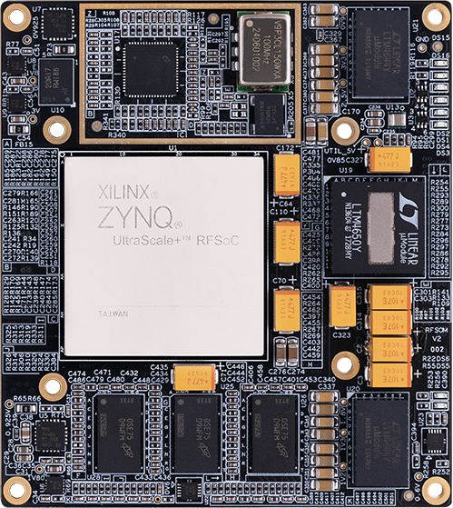
Figure 2.4.1-47DR_SoM Appearance Diagram TOP
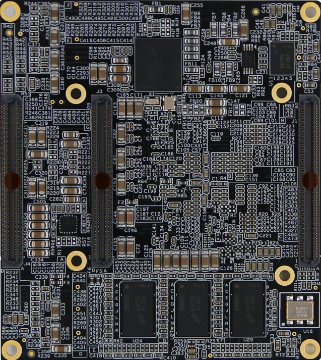
Figure 2.4.2-47DR_SoM Appearance Diagram BOTTOM
Part 3:SoM Hardware Introduction
3.1 Board Block Diagram
The core hardware block diagram of 47DR is shown in the figure:
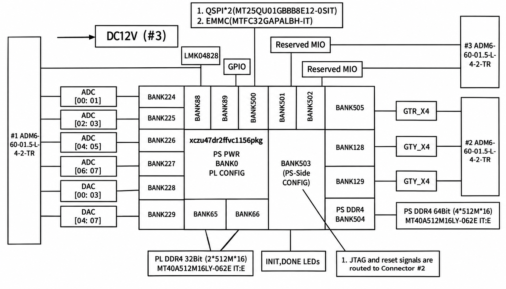
Figure 3.1.1-47DR_SoM Hardware Block Diagram
3.2 Key Parameters
The main chip of the SoM is XCZU47DR. The key parameters of the board are shown in the table below . (47DR_SoM Key Parameters)
| main chip | - XCZU47DR |
| size | - 90mm * 80.5mm |
| Expand memory | - PS DDR4 64-bit- PL DDR4 32-bit |
| storage | - Nor Flash 1Gbit *2 |
| eMMC | - PS eMMC 32 GB |
| indicator lights | - INIT_B and DONE are two working status indicator lights.- PS_ERR_OUT and PS_ERR_STATUS are two working status indicator lights. |
| Power supply for the board | The baseplate provides 12V power (via connector J4). |
| Power consumption | 60W (based on actual measured value, depending on the application) |
| Ambient temperature requirements | Operating temperature: -40℃ to 110℃ |
Table 3.2.1-47DR_SoM Key Parameters
3.3 Functions and Locations of the Board
The functions and locations of some parts of this board are shown in the figure below . The function description of each location is shown in Table 3.3.1, which shows the functions of each location on the SoM.
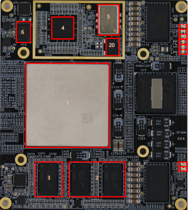
Figure 3.3.1-47DR_Core Functional Block Identification Diagram_TOP
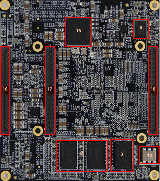
Figure 3.3.2-47DR_Core Functional Block Identification Diagram_BOTTOM
| serial number | Function |
| 1 | Main chip, XCZU47DR, reference number U1. |
| 2 | PS DDR4 extended memory , up to 2400Mb/s, 64-bit bus width, total capacity 4GB. |
| 3 | PL DDR4 extended memory , up to 2400Mb/s, 32-bit bus width, total capacity 2GB. |
| 4 | LMK04828. |
| 5 | 100MHz crystal oscillator, LMK04828 OSCIN input clock. |
| 6 | QSPI Flash, 2Gbit capacity, stores code and data, U10 and U11. |
| 7 | Main chip operating status indicator, PS_ERR_OUT. |
| 8 | Main chip operating status indicator, PS_ERR_STATUS. |
| 9 | Main chip operating status indicator, PS_INIT_B. |
| 10 | Main chip operating status indicator, PS_DONE. |
| 11 | LMK04828 data output indicator. |
| 12 | LMK04828 Status LED. |
| 13 | 12V power supply is on and functioning normally. |
| 14 | Reset indicator light. |
| 15 | EMMC. |
| 16 | GTY BANK signal expansion interface, J4. |
| 17 | PS_MIO signal extension interface, J3. |
| 18 | RF expansion interface, J1. |
| 19 | 300MHz clock speed , used as the extended DDR4 operating clock reference. |
| 20 | 10MHz clock, LMK04828 OSCOUT input clock. |
Table 3.3.1-47DR_SoM Function Description
3.4 Startup Mode
The board has four boot modes: JTAG mode, QSPI mode, SD card mode, and EMMC mode. The boot mode of the XCZU47DR can be configured via a DIP switch (which needs to be reserved on the carrier board).
The main chip of this board, XCZU47DR (reference number U1), is an RFSoC FPGA. The boot mode is determined by the high/low states of four pins: PS_MODE0, PS_MODE1, PS_MODE2, and PS_MODE3. The board uses a four-position switch (reserved on the carrier board) to select the device configuration mode. Table 3.4.1 shows the configuration modes corresponding to each state of the XCZU47DR.
| BOOT mode | Mode pin [3:0] | SW[4:1] |
| JTAG | 0000 | ON, ON, ON, ON |
| QSPI | 0010 | ON, ON, OFF, ON |
| eMMC | 0110 | ON, OFF, OFF, ON |
| SD | 0101 | ON, OFF, ON, OFF |
Table 3.4.1 - Correspondence of Mode Pins on the PS Terminal of XCZU47DR
3.5 DDR4 memory
As shown in the 47DR SoM hardware block diagram, the main chip XCZU47DR of this board is configured with two sets of DDR4 extended memory. Four DDR4 chips are installed on the PS side to form a 64-bit data bus width, and two DDR4 chips are installed on the PL side to form a 32-bit data bus width. It consists of six Micron MT40A512M16LY-062E IT:E chips. A 300MHz differential crystal oscillator is used as the reference clock. The specific DDR4 configuration on the PS and PL sides is shown in the table below :
| Location | Position | Chip Model | capacity | factory |
| PS | U24, U25, U26, U27 | MT40A512M16LY-062E IT:E | 512x16bit | Micron |
| PL | U28, U29 | MT40A512M16LY-062E IT:E | 512x16bit | Micron |
Table 3.5.1 - DDR4 Configuration
The hardware connection method for DDR4 on the PS side is shown in the following figure:
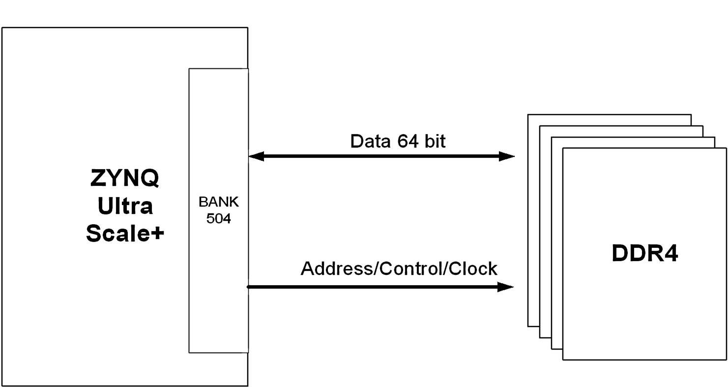
Figure 3.5.1 - Schematic diagram of DDR4 connection on the PS side
The hardware connection method for DDR4 on the PL side is as follows:
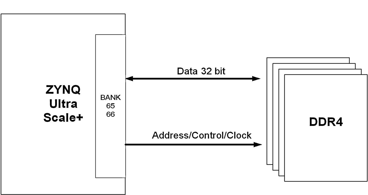
Figure 3.5.2 - Schematic diagram of DDR4 connection at the PL end
Notice:
While memory chips support transfer rates up to 3200 MT/s, FPGA chips support a maximum transfer rate of 2400 Mb/s. Please refer to the chip datasheet for details.
This section shows the highest performance parameters for the memory and main chip (which also means the highest power consumption). Users can adjust these parameters according to their usage scenarios to balance power consumption and performance .
3.6 QSPI FLASH
The board is equipped with two MT25QU01GBBB8E12-0SIT serial Nor Flash memory chips in the PS, which can be used to store executable code and data, such as bootloaders, operating systems, and bitstreams. The two QSPI chips are connected in parallel.
To achieve higher performance, two Quad-SPI devices are connected in parallel, providing a total of 8 bits of data bus for booting and configuration. The XCZU47DR is connected to two QSPI Nor Flash chips , as shown below:
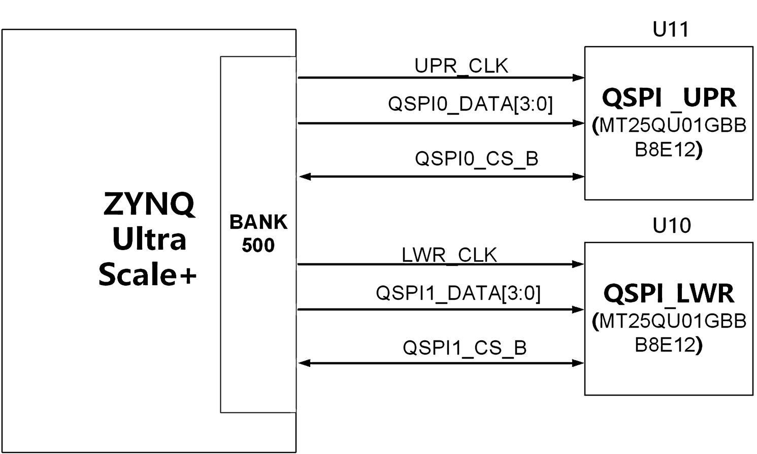
Figure 3.6.1 - Schematic diagram of interconnection between two QSPI Nor Flash chips and XCZU47DR
The interconnect pin definitions for the two QSPI Nor Flash chips are as follows :
| FPGA pin numbers | FPGA pin names | signal name | QSPI pin numbers | QSPI pin names |
| U1.MIO12_B15 | PS_MIO12_B15 | MIO12_QSPI_UPR_CLK | U11.B2 | C |
| U1.MIO10_C15 | PS_MIO10_C15 | MIO10_QSPI_UPR_DQ2 | U11.C4 | DQ2_W_B |
| U1.MIO9_F15 | PS_MIO9_F15 | MIO9_QSPI_UPR_DQ1 | U11.D2 | DQ1 |
| U1.MIO8_E15 | PS_MIO8_E15 | MIO8_QSPI_UPR_DQ0 | U11.D3 | DQ0 |
| U1. MIO11_G16 | PS_MIO11_G16 | MIO11_QSPI_UPR_DQ3 | U11.D4 | DQ3_RST_HLD_B |
| U1.MIO7_K17 | PS_MIO7_K17 | MIO7_QSPI_UPR_CS_B | U11.C2 | S_B |
| U1.MIO5_H18 | PS_MIO5_H18 | MIO5_QSPI_LWR_CS_B | U10.C2 | S_B |
| U1.MIO4_G15 | PS_MIO4_G15 | MIO4_QSPI_LWR_DQ0 | U10.D3 | DQ0 |
| U1.MIO3_K16 | PS_MIO3_K16 | MIO3_QSPI_LWR_DQ3 | U10.D4 | DQ3_RST_HLD_B |
| U1.MIO2_J16 | PS_MIO2_J16 | MIO2_QSPI_LWR_DQ2 | U10.C4 | DQ2_W_B |
| U1.MIO1_J18 | PS_MIO1_J18 | MIO1_QSPI_LWR_DQ1 | U10.D2 | DQ1 |
| U1.MIO0_J17 | PS_MIO0_J17 | MIO0_QSPI_LWR_CLK | U10.B2 | C |
Table 3.6.1 - Interconnect Pin Definitions for Two QSPI Nor Flash Chips
3.7 eMMC
The SoM provides eMMC storage. It connects to the PS terminal of the main chip and interacts directly with the main chip.
The overall connection diagram of eMMC is shown in the figure below:
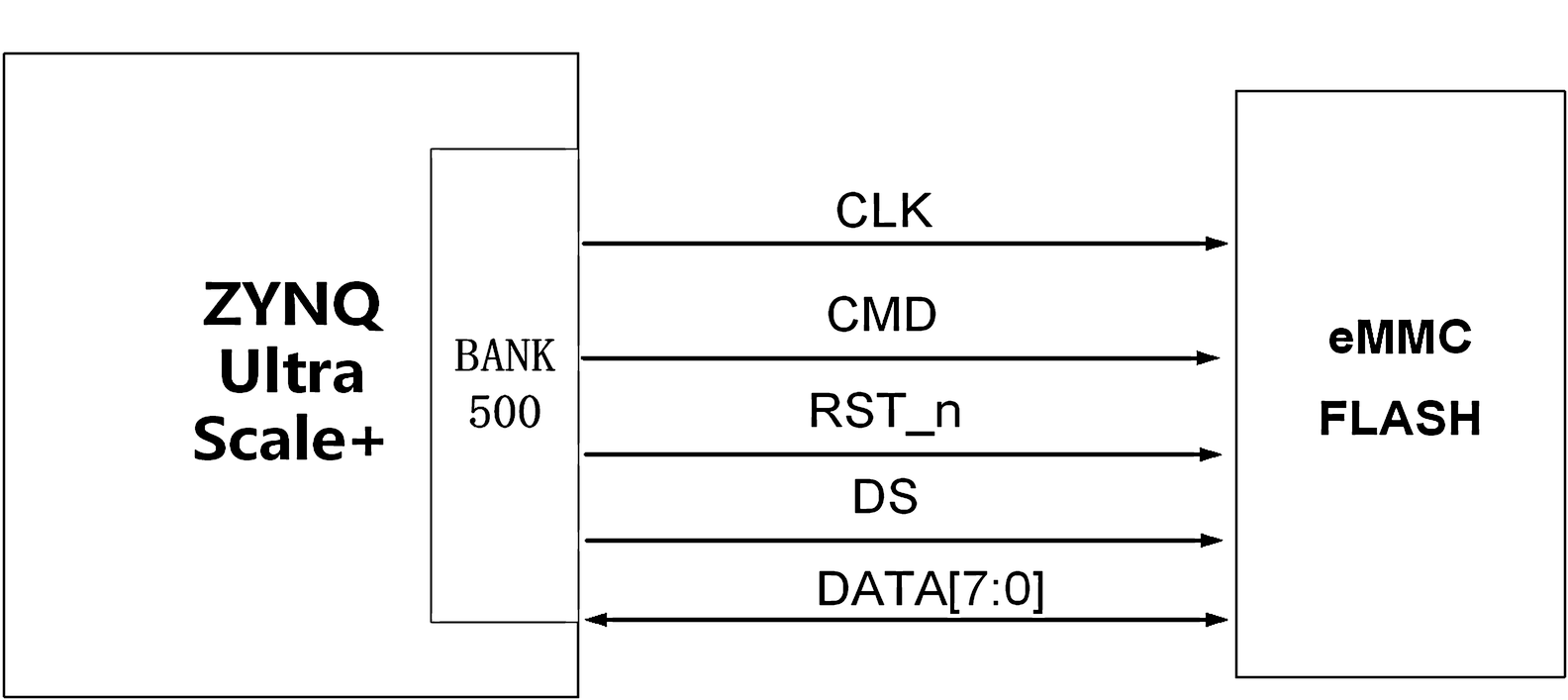
Figure 3.7.1 - Overall connection diagram of eMMC
eMMC Pin Assignment Table:
| Signal name | pin name | pin number |
| eMMC_DS | PS_MIO25_B17 | B17 |
| MIO23_eMMC_RST | PS_MIO23_D17 | D17 |
| MIO22_eMMC_CLK | PS_MIO22_E17 | E17 |
| MIO21_eMMC_CMD | PS_MIO21_F17 | F17 |
| MIO20_eMMC_DAT7 | PS_MIO20_B16 | B16 |
| MIO20_eMMC_DAT6 | PS_MIO19_C16 | C16 |
| MIO18_eMMC_DAT5 | PS_MIO18_F18 | F18 |
| MIO17_eMMC_DAT4 | PS_MIO17_E16 | E16 |
| MIO16_eMMC_DAT3 | PS_MIO16_G17 | G17 |
| MIO15_eMMC_DAT2 | PS_MIO15_D16 | D16 |
| MIO14_eMMC_DAT1 | PS_MIO14_A15 | A15 |
| MIO13_eMMC_DAT0 | PS_MIO13_G18 | G18 |
Table 3.7.1 - eMMC Pin Assignment
3.8 EEPROM
The SoM features an onboard EEPROM, model M24C08-RDW6TP, with a capacity of 8Kb, which communicates with the PL terminal via the IIC bus. EEPROM pin assignment table:
| Signal name | pin name | pin number | Remark |
| IIC_EEPROM_SCL | IO_L12N_AD8N_88_A12 | A12 | I2C clock signal |
| IIC_EEPROM_SDA | IO_L12P_AD8P_88_B12 | B12 | I2C data signal |
Table 3.8.1 - EEPROM Pin Definitions
3.9 SoM Indicator Lights
Main chip status indicator:
The main chip XCZU47DR (reference number U1) on this board has 8 status indicator lights . The positions of the FPGA status indicator lights are shown in the following figure , and the position diagram of the main chip XCZU47DR status indicator lights is also shown:
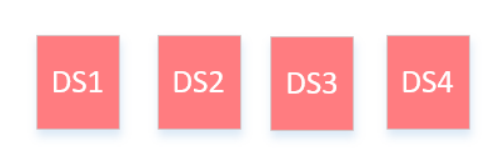
Figure 3.9.1 - Schematic diagram of the location of status indicator lights on the main chip XCZU47DR
The functional status indicated by each LED is shown in the following table, XCZU47DR Status Indicator Function Description:
| LED number | Indicator light color | Function |
| DS1 | red | FPGA initialization error |
| DS2 | red | FPGA download error |
| DS3 | red | PS_ERR_OUT indicator light |
| DS4 | red | PS_ERR_STATUS indicator light |
Table 3.9.1 - Function Description of Status Indicator Lights on Main Chip XCZU47DR
Power indicator light for the entire board:
This board requires a 12V input power supply, provided by the carrier board and introduced to the SoM via connector J4. When the input power is normal, the power indicator DS6 will be highlighted green. The DS6 indicator is located at position 13. A schematic diagram of the DS6 power indicator's location is shown in the following figure:
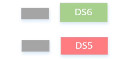
Figure 3.9.2 - Schematic diagram of the location of power indicator DS6 at position 13.
3.10 PS - GTR Interface
The PS-side GTR high-speed BANK on the SoM is not used at all; it is all pulled out through the connector. It supports a maximum data rate of 6.0Gb/s and can be used as a PCIe Gen2 x1, x2, or x4 port, or as a SATA port, supporting data rates of 1.5Gb/s, 3.0Gb/s, and 6Gb/s. It can also support DP interfaces, USB 3.0 interfaces, and other applications.
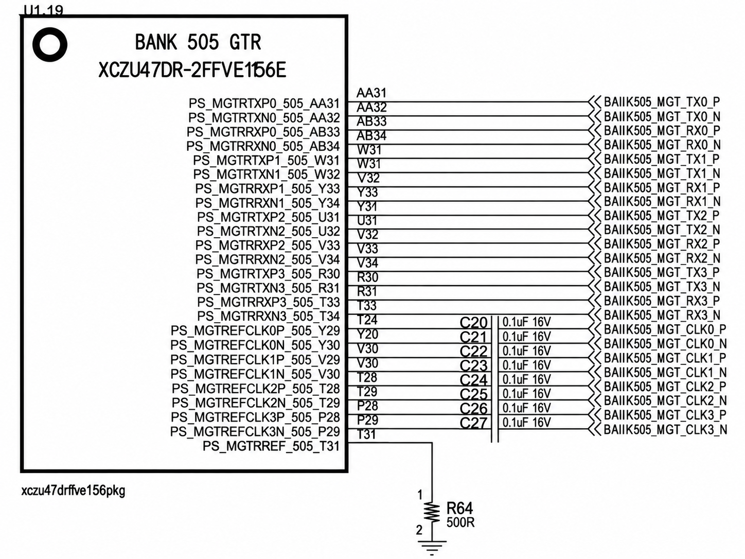
Figure 3.10.1 - Mapping diagram of GTR high-speed transceiver at PS end
3.11 PS - GTY Interface
The SoM supports the GTY high-speed transceiver, which enables PCIe x8 Gen4.0 (requires a PCIe carrier card) with data rates up to 16.0Gb/s. It also supports 100G fiber optic interface interconnection . This facilitates secondary development by users, minimizes design risks, and offers flexibility.
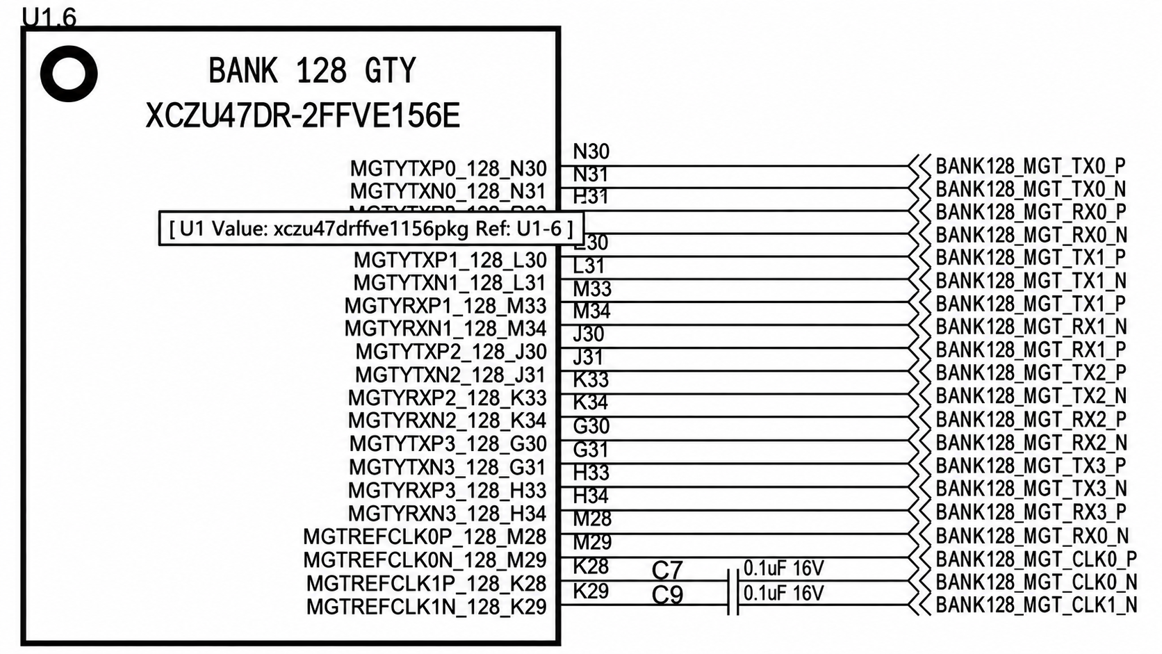
Figure 3.11.1 - High-speed transceiver mapping diagram
3.12 RF Interface
The FPGA chip used in the SoM is the Zynq™ UltraScale+™ RFSoC Gen3 series, the industry's only single-chip adaptive radio platform. The chip integrates a 14-bit RF-ADC with a maximum sampling rate of 5GSPS, and the VCM signal is also brought out to the connector for easy adjustment of the common-mode voltage.
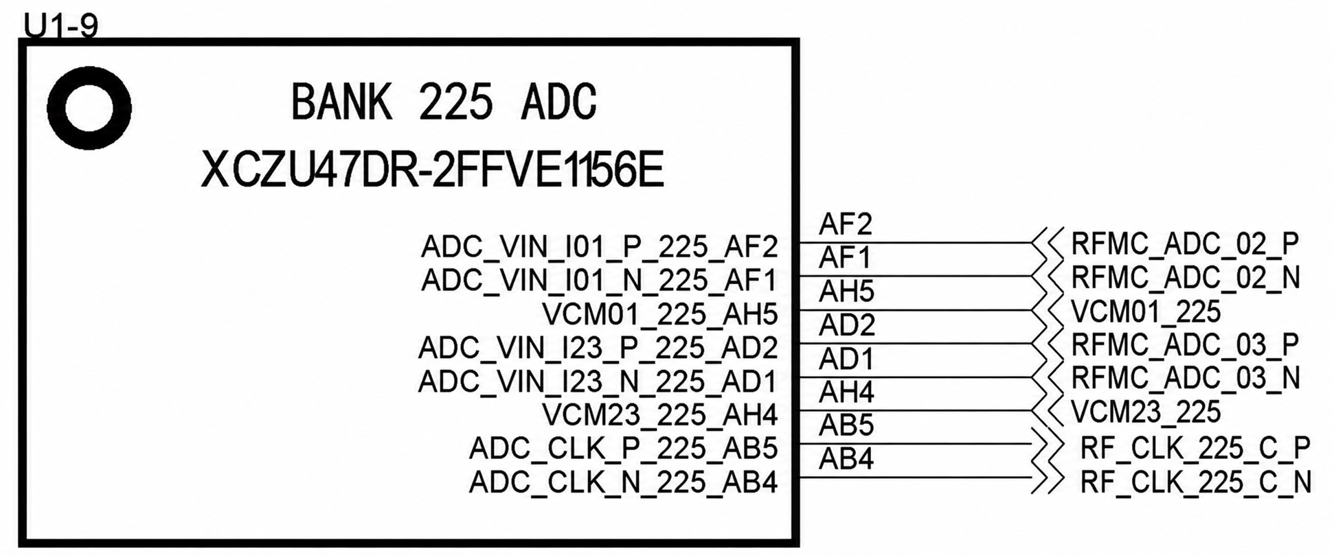
Figure 3.12.1 - RF-ADC Interface Diagram
The core component uses an FPGA chip, the Zynq™ UltraScale+™ RFSoC Gen3 series, which is the industry's only single-chip adaptive radio platform. The chip integrates a 14-bit RF-DAC with a maximum sampling rate of 9.85 GSPS.
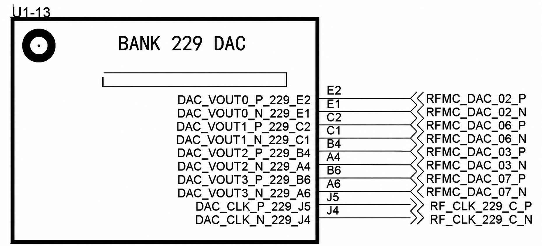
Figure 3.12.2- RF-DAC Interface Diagram
3.13 Clock Configuration
The SoM provides dual crystal clocks, with the system clock using a 33.3333MHz active crystal oscillator by default. The crystal operates at 32.768kHz and drives the internal RTC circuitry of the SoM. A schematic diagram of the clock circuit design is shown below:
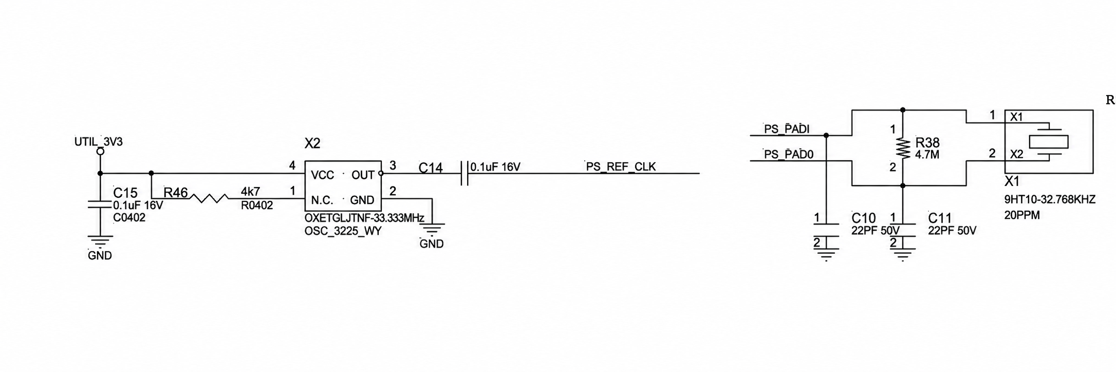
Figure 3.13.1 - Crystal Oscillator Schematic Diagram
The SoM uses the LMK04828 clock chip to distribute the clock required by each module, and the main crystal oscillator is a 100MHz crystal oscillator. It supports GTY clock recovery, external reference clock input, and SYSREF input, and can realize the parallel connection of multiple modules to form a larger-scale coherent RF channel .
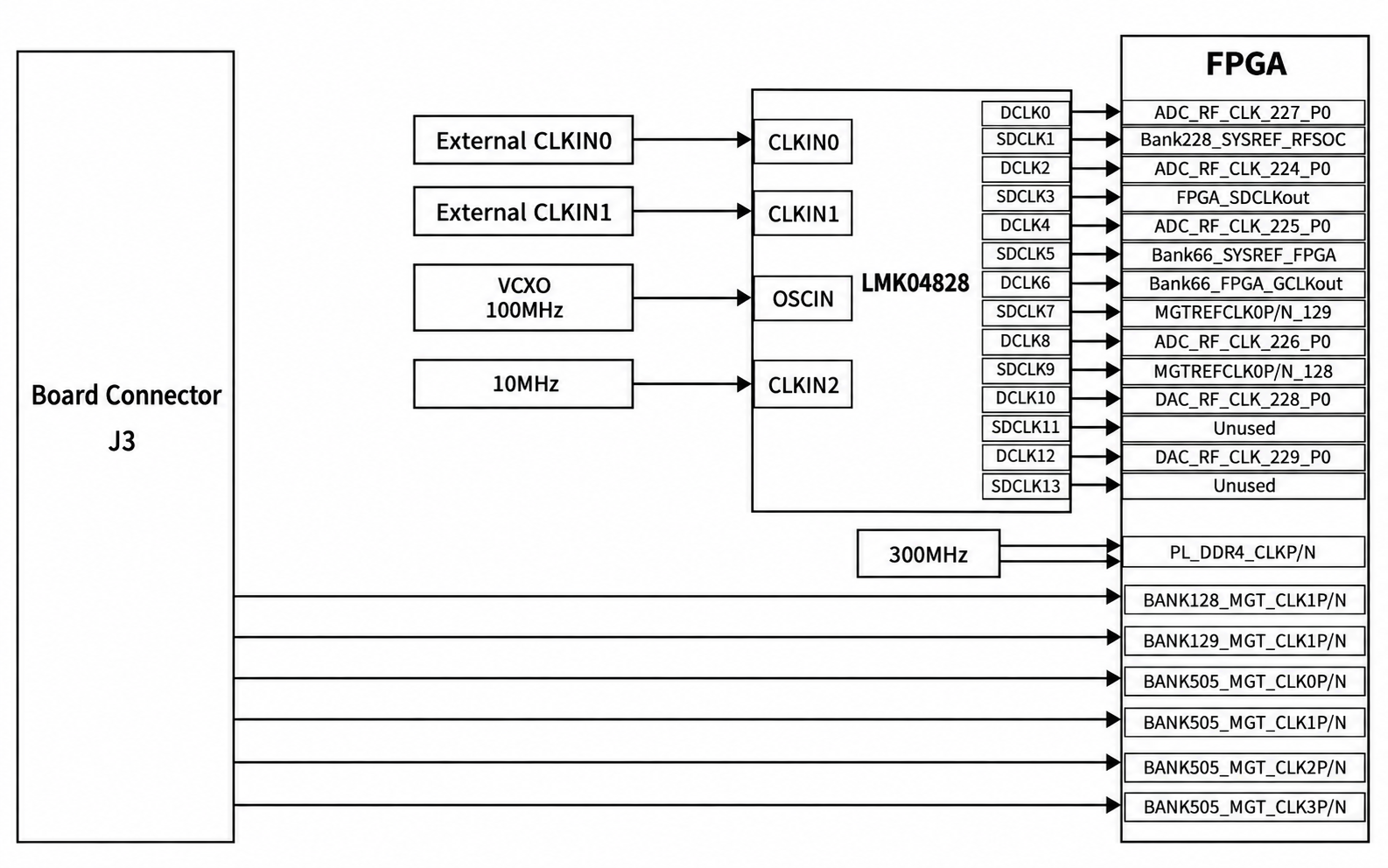
Figure 3.13.2 - Schematic diagram of the overall clock topology
3.14 Power Supply
The SoM is powered by 12V DC, supplied via a connector backplane. The typical power consumption of the SoM is 60W . The 12V system power supply is converted into different voltages by a buck regulator to drive the FPGA and other circuits on the board. The ADC and DAC on the board are powered by a linear low-voltage LDO, which has good power supply rejection (PSRR).
The extended IO BANK interface levels of the core module are as follows :
| BANK | Level | Remark |
| BANK65 | 1.2V | Without any definition, the remaining I/O is pulled to the connector. |
| BANK88 | 3.3V | HD_BANK supports 1.2~3.3V (HD I/O only) at ±5% |
| BANK89 | 1.8V or 3.3V | The SoM defaults to 1.8V, and the bank level can be adjusted using a ferrite bead. |
| BANK128 | MGTY (1.2V) | PCIe Gen4 signal |
| BANK129 | MGTY (1.2V) | PCIe Gen4 signal |
| BANK501 | 1.8V or 3.3V | The SoM defaults to 1.8V, and the bank level can be adjusted using a ferrite bead. |
| BANK502 | 1.8V or 3.3V | The SoM defaults to 1.8V, and the bank level can be adjusted using a ferrite bead. |
| BANK503 | 1.8V fixed | Configure pin outputs, mode selection, and system reset signal. |
| BANK505 | PS_MGTR | Without any definition, all high-speed signal pins and clock signals are pulled out to the connector. |
Table 3.14.1 - Main Chip XCZU47DR IO BANK Level Description
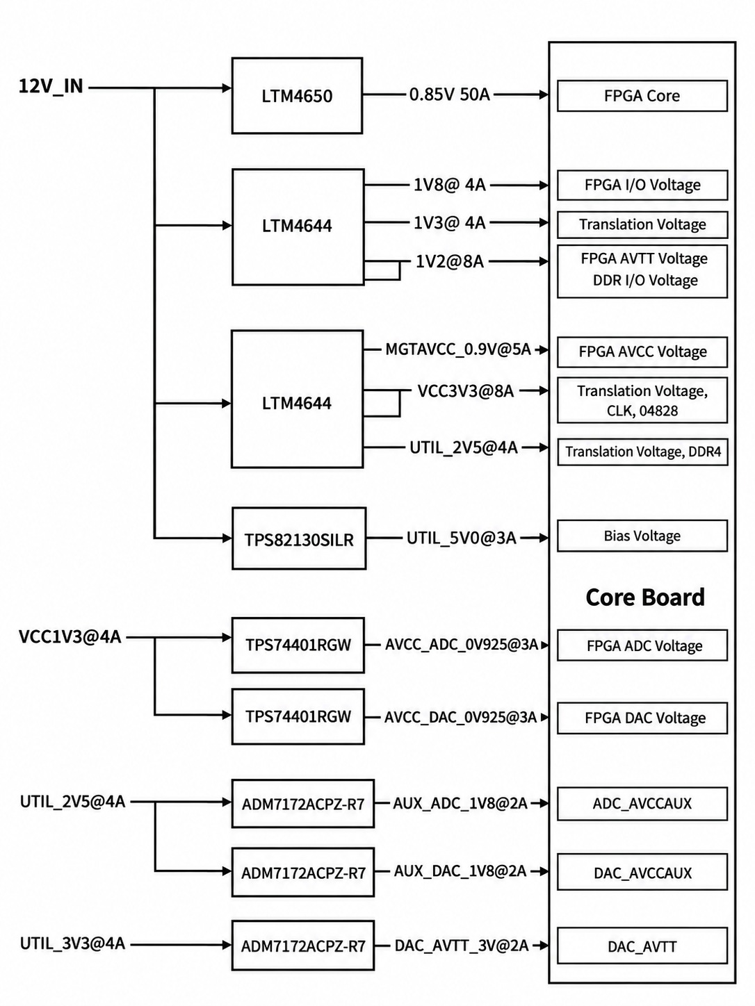
Figure 3.14.1 - Overall power supply structure tree
3.15 Structural Diagram
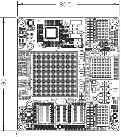
Figure 3.15.1 - Front view of the core plate
3.16 User Extension Interface Definition
The SoM has three high-speed expansion ports, connected to the carrier board via 240-pin inter-board connectors (J1, J3, J4). The connectors used are Samtec ADM6-60-01.5-L-4-2-TR connectors. The connector signal definitions are as follows:
J1 connector definition:
| label | Signal Network | label | Signal Network | label | Signal Network | label | Signal Network |
| A01 | GND | B01 | GND | C01 | GND | D01 | GND |
| A02 | GND | B02 | GND | C02 | GND | D02 | GND |
| A03 | GND | B03 | GND | C03 | GND | D03 | GND |
| A04 | GND | B04 | GND | C04 | GND | D04 | GND |
| A05 | GND | B05 | GND | C05 | GND | D05 | GND |
| A06 | VCM01_224 | B06 | VCM01_225 | C06 | VCM01_226 | D06 | VCM01_227 |
| A07 | GND | B07 | GND | C07 | GND | D07 | GND |
| A08 | GND | B08 | GND | C08 | GND | D08 | GND |
| A09 | GND | B09 | GND | C09 | GND | D09 | GND |
| A10 | GND | B10 | GND | C10 | GND | D10 | GND |
| A11 | VCM23_224 | B11 | VCM23_225 | C11 | VCM23_226 | D11 | VCM23_227 |
| A12 | GND | B12 | GND | C12 | GND | D12 | GND |
| A13 | GND | B13 | GND | C13 | GND | D13 | GND |
| A14 | GND | B14 | GND | C14 | GND | D14 | GND |
| A15 | GND | B15 | GND | C15 | GND | D15 | GND |
| A16 | RFMC_ADC_01_N | B16 | RFMC_ADC_01_P | C16 | RFMC_ADC_00_N | D16 | RFMC_ADC_00_P |
| A17 | GND | B17 | GND | C17 | GND | D17 | GND |
| A18 | GND | B18 | GND | C18 | GND | D18 | GND |
| A19 | GND | B19 | GND | C19 | GND | D19 | GND |
| A20 | GND | B20 | GND | C20 | GND | D20 | GND |
| A21 | RFMC_ADC_03_N | B21 | RFMC_ADC_03_P | C21 | RFMC_ADC_02_N | D21 | RFMC_ADC_02_P |
| A22 | GND | B22 | GND | C22 | GND | D22 | GND |
| A23 | GND | B23 | GND | C23 | GND | D23 | GND |
| A24 | GND | B24 | GND | C24 | GND | D24 | GND |
| A25 | GND | B25 | GND | C25 | GND | D25 | GND |
| A26 | RFMC_ADC_05_N | B26 | RFMC_ADC_05_P | C26 | RFMC_ADC_04_N | D26 | RFMC_ADC_04_P |
| A27 | GND | B27 | GND | C27 | GND | D27 | GND |
| A28 | GND | B28 | GND | C28 | GND | D28 | GND |
| A29 | GND | B29 | GND | C29 | GND | D29 | GND |
| A30 | GND | B30 | GND | C30 | GND | D30 | GND |
| A31 | RFMC_ADC_07_N | B31 | RFMC_ADC_07_P | C31 | RFMC_ADC_06_N | D31 | RFMC_ADC_06_P |
| A32 | GND | B32 | GND | C32 | GND | D32 | GND |
| A33 | GND | B33 | GND | C33 | GND | D33 | GND |
| A34 | GND | B34 | GND | C34 | GND | D34 | GND |
| A35 | GND | B35 | GND | C35 | GND | D35 | GND |
| A36 | RFMC_DAC_04_N | B36 | RFMC_DAC_04_P | C36 | RFMC_DAC_00_N | D36 | RFMC_DAC_00_P |
| A37 | GND | B37 | GND | C37 | GND | D37 | GND |
| A38 | GND | B38 | GND | C38 | GND | D38 | GND |
| A39 | GND | B39 | GND | C39 | GND | D39 | GND |
| A40 | GND | B40 | GND | C40 | GND | D40 | GND |
| A41 | RFMC_DAC_05_N | B41 | RFMC_DAC_05_P | C41 | RFMC_DAC_01_N | D41 | RFMC_DAC_01_P |
| A42 | GND | B42 | GND | C42 | GND | D42 | GND |
| A43 | GND | B43 | GND | C43 | GND | D43 | GND |
| A44 | GND | B44 | GND | C44 | GND | D44 | GND |
| A45 | GND | B45 | GND | C45 | GND | D45 | GND |
| A46 | RFMC_DAC_06_N | B46 | RFMC_DAC_06_P | C46 | RFMC_DAC_02_N | D46 | RFMC_DAC_02_P |
| A47 | GND | B47 | GND | C47 | GND | D47 | GND |
| A48 | GND | B48 | GND | C48 | GND | D48 | GND |
| A49 | GND | B49 | GND | C49 | GND | D49 | GND |
| A50 | GND | B50 | GND | C50 | GND | D50 | GND |
| A51 | RFMC_DAC_07_N | B51 | RFMC_DAC_07_P | C51 | RFMC_DAC_03_N | D51 | RFMC_DAC_03_P |
| A52 | GND | B52 | GND | C52 | GND | D52 | GND |
| A53 | GND | B53 | GND | C53 | GND | D53 | GND |
| A54 | GND | B54 | GND | C54 | GND | D54 | GND |
| A55 | GND | B55 | GND | C55 | GND | D55 | GND |
| A56 | GND | B56 | GND | C56 | GND | D56 | GND |
| A57 | GND | B57 | GND | C57 | GND | D57 | GND |
| A58 | GND | B58 | GND | C58 | GND | D58 | GND |
| A59 | GND | B59 | GND | C59 | GND | D59 | GND |
| A60 | GND | B60 | GND | C60 | GND | D60 | GND |
Table 3.16.1 - Signal Interconnection Table between Expansion Interface J1 and Main Chip
J3 connector definition:
| label | Signal Network | label | Signal Network | label | Signal Network | label | Signal Network |
| A01 | GND | B01 | GND | C01 | GND | D01 | GND |
| A02 | GND | B02 | GND | C02 | GND | D02 | GND |
| A03 | GND | B03 | GND | C03 | GND | D03 | GND |
| A04 | GND | B04 | GND | C04 | GND | D04 | GND |
| A05 | CLKIN0_P | B05 | CLKIN0_N | C05 | CLKIN1_P | D05 | CLKIN1_N |
| A06 | GND | B06 | GND | C06 | GND | D06 | GND |
| A07 | GND | B07 | GND | C07 | GND | D07 | GND |
| A08 | GND | B08 | GND | C08 | IO_L2P_T0L_N2_66_AP6_1V2 | D08 | IO_L2N_T0L_N3_66_AP5_1V2 |
| A09 | GND | B09 | IO_T3U_N12_66_AH12_1V2 | C09 | GND | D09 | GND |
| A10 | GND | B10 | GND | C10 | IO_L3P_T0L_N4_AD15P_66_AM6_1V2 | D10 | IO_L3N_T0L_N5_AD15N_66_AM5_1V2 |
| A11 | VCC_PSBATT_C | B11 | PS_DONE | C11 | GND | D11 | GND |
| A12 | GND | B12 | GND | C12 | GND | D12 | PS_ERR_OUT |
| A13 | GND | B13 | GND | C13 | GND | D13 | GND |
| A14 | JTAG_TDO | B14 | GND | C14 | IO_L5P_T0U_N8_AD14P_66_AP3_1V2 | D14 | IO_L5N_T0U_N9_AD14N_66_AP2_1V2 |
| A15 | GND | B15 | PS_INIT_B | C15 | GND | D15 | GND |
| A16 | GND | B16 | GND | C16 | PS_ERR_STATUS | D16 | PS_PROG_B |
| A17 | GND | B17 | GND | C17 | GND | D17 | GND |
| A18 | PS_POR_B | B18 | PS_SRST_B | C18 | GND | D18 | GND |
| A19 | GND | B19 | GND | C19 | IO_L1P_T0L_N0_DBC_66_AP8_1V2 | D19 | IO_L1N_T0L_N1_DBC_66_AP7_1V2 |
| A20 | JTAG_TCK | B20 | JTAG_TMS | C20 | GND | D20 | GND |
| A21 | GND | B21 | GND | C21 | IO_L6P_T0U_N10_AD6P_66_AN2_1V2 | D21 | IO_L6N_T0U_N11_AD6N_66_AN1_1V2 |
| A22 | IO_L4P_T0U_N6_DBC_AD7P_66_AN5_1V2 | B22 | IO_L4N_T0U_N7_DBC_AD7N_66_AN4_1V2 | C22 | GND | D22 | GND |
| A23 | GND | B23 | GND | C23 | GND | D23 | GND |
| A24 | PS_MODE3 | B24 | JTAG_TDI | C24 | GND | D24 | GND |
| A25 | GND | B25 | GND | C25 | PS_MODE2 | D25 | LMK_SYNC_C |
| A26 | PS_MODE1 | B26 | PS_MODE0 | C26 | GND | D26 | GND |
| A27 | GND | B27 | GND | C27 | GND | D27 | GND |
| A28 | GND | B28 | GND | C28 | BANK505_MGT_RX0_P | D28 | BANK505_MGT_RX0_N |
| A29 | BANK505_MGT_CLK0_P | B29 | BANK505_MGT_CLK0_N | C29 | GND | D29 | GND |
| A30 | GND | B30 | GND | C30 | BANK505_MGT_RX1_P | D30 | BANK505_MGT_RX1_N |
| A31 | BANK505_MGT_TX0_P | B31 | BANK505_MGT_TX0_N | C31 | GND | D31 | GND |
| A32 | GND | B32 | GND | C32 | BANK505_MGT_RX2_P | D32 | BANK505_MGT_RX2_N |
| A33 | BANK505_MGT_TX1_P | B33 | BANK505_MGT_TX1_N | C33 | GND | D33 | GND |
| A34 | GND | B34 | GND | C34 | BANK505_MGT_RX3_P | D34 | BANK505_MGT_RX3_N |
| A35 | BANK505_MGT_TX2_P | B35 | BANK505_MGT_TX2_N | C35 | GND | D35 | GND |
| A36 | GND | B36 | GND | C36 | BANK505_MGT_CLK1_P | D36 | BANK505_MGT_CLK1_N |
| A37 | BANK505_MGT_CLK2_P | B37 | BANK505_MGT_CLK2_N | C37 | GND | D37 | GND |
| A38 | GND | B38 | GND | C38 | BANK505_MGT_CLK3_P | D38 | BANK505_MGT_CLK3_N |
| A39 | BANK505_MGT_TX3_P | B39 | BANK505_MGT_TX3_N | C39 | GND | D39 | GND |
| A40 | GND | B40 | GND | C40 | BANK128_MGT_RX0_P | D40 | BANK128_MGT_RX0_N |
| A41 | BANK128_MGT_TX0_P | B41 | BANK128_MGT_TX0_N | C41 | GND | D41 | GND |
| A42 | GND | B42 | GND | C42 | BANK128_MGT_CLK1_P | D42 | BANK128_MGT_CLK1_N |
| A43 | BANK128_MGT_TX1_P | B43 | BANK128_MGT_TX1_N | C43 | GND | D43 | GND |
| A44 | GND | B44 | GND | C44 | BANK128_MGT_RX1_P | D44 | BANK128_MGT_RX1_N |
| A45 | BANK129_MGT_CLK1_P | B45 | BANK129_MGT_CLK1_N | C45 | GND | D45 | GND |
| A46 | GND | B46 | GND | C46 | BANK128_MGT_RX2_P | D46 | BANK128_MGT_RX2_N |
| A47 | BANK128_MGT_TX2_P | B47 | BANK128_MGT_TX2_N | C47 | GND | D47 | GND |
| A48 | GND | B48 | GND | C48 | BANK128_MGT_RX3_P | D48 | BANK128_MGT_RX3_N |
| A49 | BANK128_MGT_TX3_P | B49 | BANK128_MGT_TX3_N | C49 | GND | D49 | GND |
| A50 | GND | B50 | GND | C50 | BANK129_MGT_RX0_P | D50 | BANK129_MGT_RX0_N |
| A51 | BANK129_MGT_TX0_P | B51 | BANK129_MGT_TX0_N | C51 | GND | D51 | GND |
| A52 | GND | B52 | GND | C52 | BANK129_MGT_RX1_P | D52 | BANK129_MGT_RX1_N |
| A53 | BANK129_MGT_TX1_P | B53 | BANK129_MGT_TX1_N | C53 | GND | D53 | GND |
| A54 | GND | B54 | GND | C54 | BANK129_MGT_RX2_P | D54 | BANK129_MGT_RX2_N |
| A55 | BANK129_MGT_TX2_P | B55 | BANK129_MGT_TX2_N | C55 | GND | D55 | GND |
| A56 | GND | B56 | GND | C56 | BANK129_MGT_RX3_P | D56 | BANK129_MGT_RX3_N |
| A57 | BANK129_MGT_TX3_P | B57 | BANK129_MGT_TX3_N | C57 | GND | D57 | GND |
| A58 | GND | B58 | GND | C58 | GND | D58 | GND |
| A59 | GND | B59 | GND | C59 | GND | D59 | GND |
| A60 | GND | B60 | GND | C60 | GND | D60 | GND |
Table 3.16.2 - Signal Interconnection Table between Expansion Interface J3 and Main Chip
J4 connector definition:
| label | Signal Network | label | Signal Network | label | Signal Network | label | Signal Network |
| A01 | VCC12V_SW | B01 | VCC12V_SW | C01 | VCC12V_SW | D01 | VCC12V_SW |
| A02 | VCC12V_SW | B02 | VCC12V_SW | C02 | VCC12V_SW | D02 | VCC12V_SW |
| A03 | VCC12V_SW | B03 | VCC12V_SW | C03 | VCC12V_SW | D03 | VCC12V_SW |
| A04 | VCC12V_SW | B04 | VCC12V_SW | C04 | VCC12V_SW | D04 | VCC12V_SW |
| A05 | GND | B05 | GND | C05 | GND | D05 | GND |
| A06 | GND | B06 | GND | C06 | GND | D06 | GND |
| A07 | GND | B07 | GND | C07 | GND | D07 | GND |
| A08 | GND | B08 | GND | C08 | DXP | D08 | DXN |
| A09 | BANK501_PS_MIO28 | B09 | GND | C09 | GND | D09 | GND |
| A10 | GND | B10 | GND | C10 | BANK502_PS_MIO66 | D10 | BANK502_PS_MIO67 |
| A11 | BANK501_PS_MIO29 | B11 | BANK501_PS_MIO30 | C11 | GND | D11 | GND |
| A12 | GND | B12 | GND | C12 | BANK502_PS_MIO68 | D12 | BANK502_PS_MIO76 |
| A13 | BANK501_PS_MIO33 | B13 | BANK501_PS_MIO31 | C13 | GND | D13 | GND |
| A14 | GND | B14 | GND | C14 | BANK502_PS_MIO69 | D14 | BANK502_PS_MIO77 |
| A15 | BANK501_PS_MIO35 | B15 | BANK501_PS_MIO32 | C15 | GND | D15 | GND |
| A16 | GND | B16 | GND | C16 | BANK502_PS_MIO72 | D16 | BANK502_PS_MIO74 |
| A17 | BANK501_PS_MIO49 | B17 | BANK501_PS_MIO42 | C17 | GND | D17 | GND |
| A18 | GND | B18 | GND | C18 | BANK502_PS_MIO70 | D18 | BANK502_PS_MIO75 |
| A19 | BANK501_PS_MIO47 | B19 | BANK501_PS_MIO50 | C19 | GND | D19 | GND |
| A20 | GND | B20 | GND | C20 | BANK502_PS_MIO73 | D20 | BANK502_PS_MIO64 |
| A21 | BANK501_PS_MIO48 | B21 | BANK501_PS_MIO51 | C21 | GND | D21 | GND |
| A22 | GND | B22 | GND | C22 | BANK502_PS_MIO65 | D22 | BANK502_PS_MIO71 |
| A23 | BANK501_PS_MIO44 | B23 | BANK501_PS_MIO45 | C23 | GND | D23 | GND |
| A24 | GND | B24 | GND | C24 | BANK502_PS_MIO54 | D24 | BANK502_PS_MIO56 |
| A25 | BANK501_PS_MIO46 | B25 | BANK501_PS_MIO39 | C25 | GND | D25 | GND |
| A26 | GND | B26 | GND | C26 | BANK502_PS_MIO60 | D26 | BANK502_PS_MIO62 |
| A27 | BANK501_PS_MIO41 | B27 | BANK501_PS_MIO43 | C27 | GND | D27 | GND |
| A28 | GND | B28 | GND | C28 | BANK502_PS_MIO63 | D28 | BANK502_PS_MIO58 |
| A29 | BANK501_PS_MIO27 | B29 | BANK501_PS_MIO26 | C29 | GND | D29 | GND |
| A30 | GND | B30 | GND | C30 | BANK502_PS_MIO59 | D30 | BANK502_PS_MIO55 |
| A31 | BANK501_PS_MIO40 | B31 | BANK501_PS_MIO38 | C31 | GND | D31 | GND |
| A32 | GND | B32 | GND | C32 | BANK502_PS_MIO61 | D32 | BANK501_PS_MIO37 |
| A33 | BANK501_PS_MIO36 | B33 | BANK500_PS_MIO24 | C33 | GND | D33 | GND |
| A34 | GND | B34 | GND | C34 | BANK502_PS_MIO57 | D34 | BANK502_PS_MIO52 |
| A35 | BANK501_PS_MIO34 | B35 | BANK500_PS_MIO6 | C35 | GND | D35 | GND |
| A36 | GND | B36 | GND | C36 | BANK502_PS_MIO53 | D36 | GND |
| A37 | GND | B37 | GND | C37 | GND | D37 | GND |
| A38 | GND | B38 | GND | C38 | GND | D38 | BANK88_IO_GC_L5N |
| A39 | BANK89_IO_L10P | B39 | BANK89_IO_L10N | C39 | GND | D39 | GND |
| A40 | GND | B40 | GND | C40 | BANK89_IO_L12P | D40 | BANK89_IO_L12N |
| A41 | BANK89_IO_L9P | B41 | BANK89_IO_L9N | C41 | GND | D41 | GND |
| A42 | GND | B42 | GND | C42 | BANK89_IO_L11P | D42 | BANK89_IO_L11N |
| A43 | BANK89_IO_GC_L8P | B43 | BANK89_IO_GC_L8N | C43 | GND | D43 | GND |
| A44 | GND | B44 | GND | C44 | BANK88_IO_GC_L6P | D44 | BANK88_IO_GC_L6N |
| A45 | GND | B45 | GND | C45 | GND | D45 | GND |
| A46 | GND | B46 | GND | C46 | BANK88_IO_GC_L7P | D46 | BANK88_IO_GC_L7N |
| A47 | BANK89_IO_GC_L7P | B47 | BANK89_IO_GC_L7N | C47 | GND | D47 | GND |
| A48 | GND | B48 | GND | C48 | BANK88_IO_L9P | D48 | BANK88_IO_L9N |
| A49 | BANK89_IO_GC_L5P | B49 | BANK89_IO_GC_L5N | C49 | GND | D49 | GND |
| A50 | GND | B50 | GND | C50 | BANK88_IO_L10P | D50 | BANK88_IO_L10N |
| A51 | BANK89_IO_L4P | B51 | BANK89_IO_L4N | C51 | GND | D51 | GND |
| A52 | GND | B52 | GND | C52 | BANK88_IO_L11P | D52 | BANK88_IO_L11N |
| A53 | BANK89_IO_L2P | B53 | BANK89_IO_L2N | C53 | GND | D53 | GND |
| A54 | GND | B54 | GND | C54 | BANK88_IO_GC_L8P | D54 | BANK88_IO_GC_L8N |
| A55 | BANK89_IO_L3P | B55 | BANK89_IO_L3N | C55 | GND | D55 | GND |
| A56 | GND | B56 | GND | C56 | BANK89_IO_L1P | D56 | BANK89_IO_L1N |
| A57 | BANK89_IO_GC_L6P | B57 | BANK89_IO_GC_L6N | C57 | GND | D57 | GND |
| A58 | GND | B58 | GND | C58 | GND | D58 | GND |
| A59 | GND | B59 | GND | C59 | GND | D59 | GND |
| A60 | GND | B60 | GND | C60 | GND | D60 | GND |
Table 3.16.3 - Signal Interconnection Table between Expansion Interface J4 and Main Chip
Part 4:Carrier Board
4.1 Carrier Board Schematic Diagram
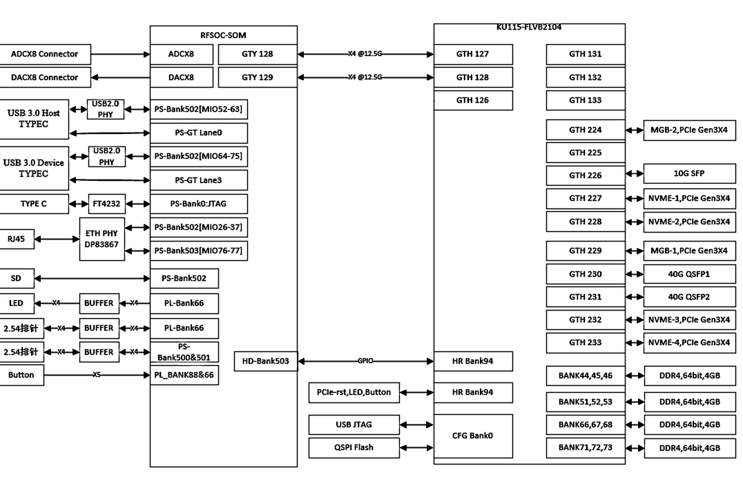
Figure 4.1.1 - Carrier plate block diagram
4.2 Key Parameters of the Carrier Plate
The carrier board is equipped with the XCKU115-FLVB2104 chip . The key parameters of the carrier board are shown in the table below :
| main chip | - XCKU115-FLVB2104 |
| size | - 215mm * 260mm |
| storage | - KU115 Extended Nor Flash 512Mb *2- The KU115 expands to include four 64-bit DDR4 modules. |
| RFSoC terminal | - USB & JTAG- USB 3.0*2- Gigabit Ethernet ports- DAC*8- ADC*8- SD Card- Status indicator lights *4- 5 buttons |
| KU115 terminal | - NVMe interfaces *4- MGB interface *2- QSFP*2- SFP+- USB & JTAG- User-defined indicator lights *8 |
| Power supply for the board | - 12V |
| Power consumption | 60W (based on actual measured value, depending on the application) |
| Ambient temperature requirements | Operating temperature: -40℃ to 110℃ |
Table 4.2.1 - Key Parameters of Carrier Plate
4.3 Functions and Locations of the Carrier Board
The functions and locations of the carrier board are shown in the following figures . Figures 4.3.1 and 4.3.2 are carrier board identification diagrams, and the functional descriptions of each location are shown in Table 4.3.1 :
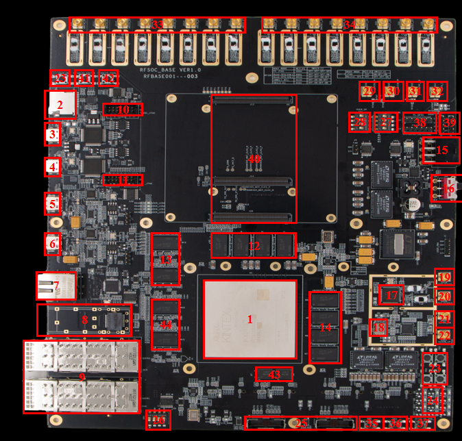
Figure 4.3.1 - Interface marking diagram on the front of the carrier board
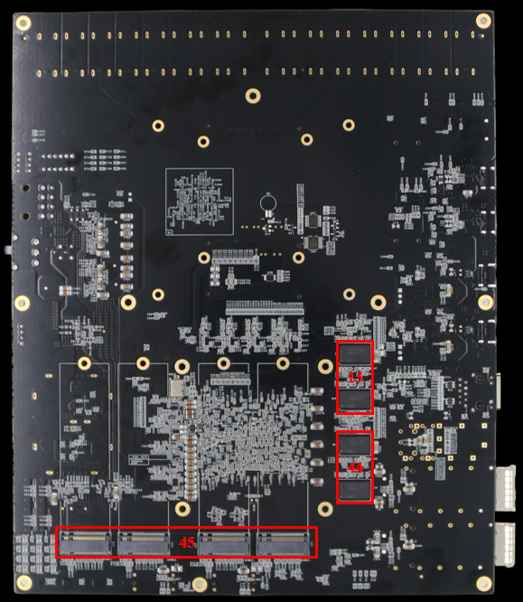
Figure 4.3.2 - Interface marking diagram on the back of the carrier plate
| serial number | Function |
| 1 | Main chip, XCKU115-FLVB2104, tag number U1. |
| 2 | RFSoC side SD card slot. |
| 3 | RFSoC side USB & JTAG, pin number J10. |
| 4 | KU115 side USB & JTAG, pin number J3. |
| 5 | RFSoC side USB 3.0, pin number J8. |
| 6 | RFSoC side USB 3.0, pin number J6. |
| 7 | RFSoC side network port. |
| 8 | KU115 side SFP mount. |
| 9 | KU115 has two QSFP cages on the side, labeled U10 and U13. |
| 10 | RFSoC side JTAG interface. |
| 11 | KU115 side JTAG interface. |
| 12 | The KU115 has a DDR4 extended memory C0 , with a maximum speed of 2666Mb/s, a 64-bit bus width, and a total capacity of 4GB. |
| 13 | The KU115 has a DDR4 extended memory C2 , with a maximum speed of 2666Mb/s, a 64-bit bus width, and a total capacity of 4GB. |
| 14 | The KU115 has a DDR4 extended memory C1 , with a maximum speed of 2666Mb/s, a 64-bit bus width, and a total capacity of 4GB. |
| 15 | Carrier board 12V power interface J27. |
| 16 | Power switch SW6. |
| 17 | Clock generator SI5341. |
| 18 | KU115 100MHz clock crystal oscillator. |
| 19 | SI5341 IN0 External Clock Input Port XS18. |
| 20 | SI5341 OUT9 clock output port XS19. |
| 21 | The SoM LMK04828 has an input clock port XS25, CLKIN1 N. |
| 22 | The SoM LMK04828 has a CLKIN1 P input clock port XS24. |
| 23 | RFSoC users can customize the buttons. |
| 24 | KU115 Side Extended LED Light. |
| 25 | KU115 side MGB1 and MGB2 connectors, tag numbers P1 and P2. |
| 26 | KU115 side mode control switch, tag number SW1. |
| 27 | RFSoC side mode control switch, tag number SW5. |
| 28 | KU115 has a reserved DIP switch SW2. |
| 29 | The SoM LMK04828 has a CLKIN0 N input clock port XS23. |
| 30 | The SoM LMK04828 has a CLKIN0 P input clock port XS22. |
| 31 | The SoM LMK04828 has a SYNC input port XS21. |
| 32 | RFSoC side PPS signal interface XS17. |
| 33 | RFSoC side ADC_IN. |
| 34 | RFSoC side DAC_OUT. |
| 35 | KU115 side reset button PB8. |
| 36 | KU115 side PROGRAM_B button PB9. |
| 37 | RFSoC side PS_POR_B button PB5. |
| 38 | RFSoC reserves I/O interfaces J11 and J12. |
| 39 | RFSoC fan interfaces J22 and J23. |
| 40 | Board-to-board connectors, tag numbers J13, J14, and J20. |
| 41 | RFSoC side PS_SRST_B button PB6. |
| 42 | RFSoC side PS_PROG_B button PB7. |
| 43 | QSPI Flash stores code and data, U7 and U8. |
| 44 | The KU115 has a DDR4 extended memory C3 , with a maximum speed of 2666Mb/s, a 64-bit bus width, and a total capacity of 4GB. |
| 45 | NVMe sockets: U18, U19, U20, U21. |
Table 4.3.1 - Functional Description of Each Position on the Carrier Board
4.4 Carrier Board Startup Mode
The carrier board has two boot modes: JTAG mode and QSPI mode. The boot mode of XCKU115-FLVB2104 can be configured by using the DIP switch SW1 .
The carrier board carries the XCKU115-FLVB2104 chip (reference number U1). The board selects the device configuration mode via switch SW1 . Table 4.4.1 shows the configuration modes corresponding to each state of the XCKU115-FLVB2104 :
| BOOT mode | Mode pin [2:0] | SW1[2:4] |
| JTAG | 101 | ON, OFF, ON |
| QSPI | 001 | OFF, OFF, ON |
Table 4.4.1 - Carrier Board XCKU115 - FLVB2104 Mode Configuration
4.5 Micro SD Card Slot
The carrier board includes a Micro SD card interface derived from the RFSoC , providing users with access to SD card storage for storing the BOOT program, Linux operating system kernel, file system, and other user data files. The SD card I/O signals are connected to the MIO signals of the PS BANK501 . A schematic diagram of the PS and SD card connector connection is shown below:
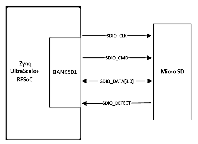
Figure 4.5.1 - SD Card Connection Diagram
SD card pin assignment:
| Signal name | pin name | pin number | Remark |
| SDIO_CLK | PS_MIO51_B21 | B21 | SD clock signal |
| SDIO_CMD | PS_MIO50_A22 | A22 | SD command signals |
| SDIO_DAT0 | PS_MIO46_A20 | A20 | SD data Bit0 |
| SDIO_DAT1 | PS_MIO47_D21 | D21 | SD data Bit1 |
| SDIO_DAT2 | PS_MIO48_C21 | C21 | SD data Bit2 |
| SDIO_DAT3 | PS_MIO49_E21 | E21 | SD data Bit3 |
| SDIO_DETECT | PS_MIO45_B20 | B20 | SD card detection signal |
Table 4.5.1 - SD Card Pin Assignment
4.6 USB 3.0 Interface
The carrier board has two USB 3.0 ports on the RFSoC side, supporting HOST and SLAVE operating modes with a data transfer rate of up to 5.0Gb/s. The USB 3.0 ports connect via the HD3SS3220IRNHT and Type-C interface, while the USB 2.0 ports connect to an external USB3320C chip via the ULPI interface , enabling high-speed data communication between USB 3.0 and USB 2.0. A USB 3.0 connection diagram is shown below:
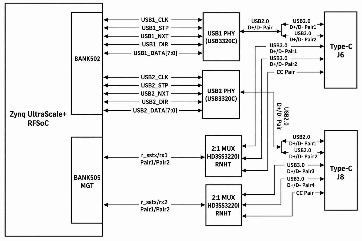
Figure 4.6.1 - Schematic diagram of USB 3.0 connection
| Signal name | pin name | ZYNQ pin number | Remark |
| r_sstxp1 | PS_MGTRTXP3_505_R30 | R30 | USB3.0 TX_P |
| r_sstxn1 | PS_MGTRTXN3_505_R31 | R31 | USB3.0 TX_N |
| r_ssrxp1 | PS_MGTRRXP3_505_T33 | T33 | USB3.0 RX_P. |
| r_ssrxn1 | PS_MGTRRXN3_505_T34 | T34 | USB3.0 RX_N |
| USB1_DATA0 | PS_MIO68_E25 | E25 | USB 2.0 data bit 0 |
| USB1_DATA1 | PS_MIO69_E24 | E24 | USB 2.0 data bit 1 |
| USB1_DATA2 | PS_MIO66_F24 | F24 | USB 2.0 data bit 2 |
| USB1_DATA3 | PS_MIO71_A24 | A24 | USB 2.0 data bit 3 |
| USB1_DATA4 | PS_MIO72_C25 | C25 | USB 2.0 data bit 4 |
| USB1_DATA5 | PS_MIO73_A25 | A25 | USB 2.0 data bit 5 |
| USB1_DATA6 | PS_MIO74_C26 | C26 | USB 2.0 data bit 6 |
| USB1_DATA7 | PS_MIO75_B26 | B26 | USB 2.0 data bit 7 |
| USB1_STP | PS_MIO70_B25 | B25 | USB 2.0 stop signal |
| USB1_DIR | PS_MIO65_C24 | C24 | USB 2.0 data direction signal |
| USB1_CLK | PS_MIO64_D24 | D24 | USB 2.0 clock signal |
| USB1_NXT | PS_MIO67_F25 | F25 | USB 2.0 Next Data Signal |
| r_sstxp2 | PS_MGTRTXP0_505_AA31 | AA31 | USB3.0 TX_P |
| r_sstxn2 | PS_MGTRTXN0_505_AA32 | AA32 | USB3.0 TX_N |
| r_ssrxp2 | PS_MGTRRXP0_505_AB33 | AB33 | USB3.0 RX_P. |
| r_ssrxn2 | PS_MGTRRXN0_505_AB34 | AB34 | USB3.0 RX_N |
| USB2_DATA0 | PS_MIO56_G23 | G23 | USB 2.0 data bit 0 |
| USB2_DATA1 | PS_MIO57_F23 | F23 | USB 2.0 data bit 1 |
| USB2_DATA2 | PS_MIO54_H23 | H23 | USB 2.0 data bit 2 |
| USB2_DATA3 | PS_MIO59_D23 | D23 | USB 2.0 data bit 3 |
| USB2_DATA4 | PS_MIO60_A23 | A23 | USB 2.0 data bit 4 |
| USB2_DATA5 | PS_MIO61_E22 | E22 | USB 2.0 data bit 5 |
| USB2_DATA6 | PS_MIO62_B23 | B23 | USB 2.0 data bit 6 |
| USB2_DATA7 | PS_MIO63_C23 | C23 | USB 2.0 data bit 7 |
| USB2_STP | PS_MIO58_B22 | B22 | USB 2.0 stop signal |
| USB2_DIR | PS_MIO53_F22 | F22 | USB 2.0 data direction signal |
| USB2_CLK | PS_MIO52_G22 | G22 | USB 2.0 clock signal |
| USB2_NXT | PS_MIO55_D22 | D22 | USB 2.0 Next Data Signal |
Table 4.6.1 - USB Interface Pin Assignment
4.7 Gigabit Ethernet Interface
The carrier board has one Gigabit Ethernet interface connected to the RFSoC PS end. The Ethernet chip used is the TEXAS INSTRUMENTS DP83867IRRGZ chip, providing network communication services to the user. The Ethernet PHY chip on the PS end is connected to the MIO of the ZYNQ PS end BANK501. The DP83867IRRGZ chip supports 10/100/1000 Mbps network transmission rates and communicates with the ZYNQ system's MAC layer via the RGMII interface. A schematic diagram of the Gigabit Ethernet PHY chip connection is shown below :
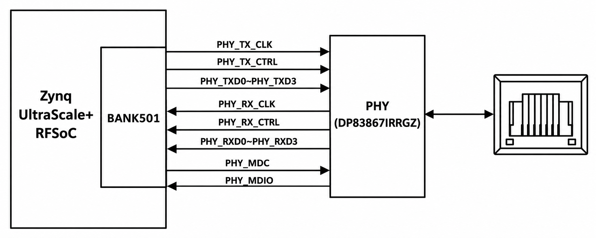
Figure 4.7.1 - Schematic diagram of Ethernet connection
| Signal name | pin name | pin number | PHY chip | |
| pin number | pin name | |||
| ENET_TX_CLK | PS_MIO26_K19 | K19 | 29 | TX_CLK |
| ENET_TX_D0 | PS_MIO27_H19 | H19 | 28 | TXD0 |
| ENET_TX_D1 | PS_MIO28_J19 | J19 | 27 | TXD1 |
| ENET_TX_D2 | PS_MIO29_H21 | H21 | 26 | TXD2 |
| ENET_TX_D3 | PS_MIO30_H20 | H20 | 25 | TXD3 |
| ENET_TX_CTRL | PS_MIO31_G20 | G20 | 37 | TX_CTRL |
| ENET_RX_CLK | PS_MIO32_F19 | F19 | 32 | RXCLK |
| ENET_RX_D0 | PS_MIO33_G21 | G21 | 33 | RXD0 |
| ENET_RX_D1 | PS_MIO34_D18 | D18 | 34 | RXD1 |
| ENET_RX_D2 | PS_MIO35_F20 | F20 | 35 | RXD2 |
| ENET_RX_D3 | PS_MIO36_C18 | C18 | 36 | RXD3 |
| ENET_RX_CTRL | PS_MIO37_E19 | E19 | 38 | RX_CTRL |
| ENET_MDC | PS_MIO76_E26 | E26 | 16 | MDC |
| ENET_MDIO | PS_MIO77_D26 | D26 | 17 | MDIO |
| ENET_RESET_B(MIO41_ETH_RESET#) | PS_MIO41_C19 | C19 | 43 | RESET_B |
| PS_POR_B | PS_POR_B_N24 | N24 | ||
Table 4.7.1 - PHY to XCZU47DR Pin Assignment
4.8 JTAG & UART
The carrier board has two JTAG & UART interfaces reserved, one for the SoM RFSoC (J10) and the other for the KU115 (J3), used for downloading and debugging FPGA programs or burning programs to FLASH. We used FTDI's 5th generation USB device chip, the FT4232HL-REEL , which is a USB 2.0 high-speed to UART/FIFO chip with two multi-protocol synchronous serial engines allowing JTAG. It has the capability to be configured with various industry-standard serial or parallel interfaces. The JTAG & UART connection diagram is shown below :
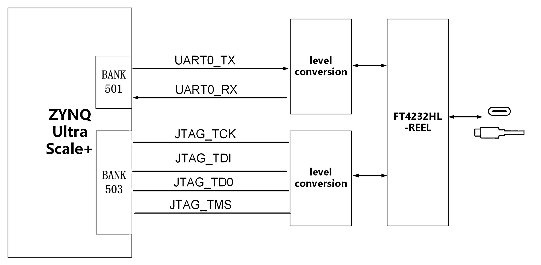
Figure 4.8.1- RFSoC side JTAG & UART connector connection diagram
| Signal name | pin name | pin number | Remark |
| UART0_RXD_MIO39_TXD | PS_MIO39_D19 | D19 | PS UART data output |
| UART0_TXD_MIO38_RXD | PS_MIO38_B18 | B18 | PS UART data input |
Table 4.8.1 - RFSoC Side JTAG & UART Pin Assignment
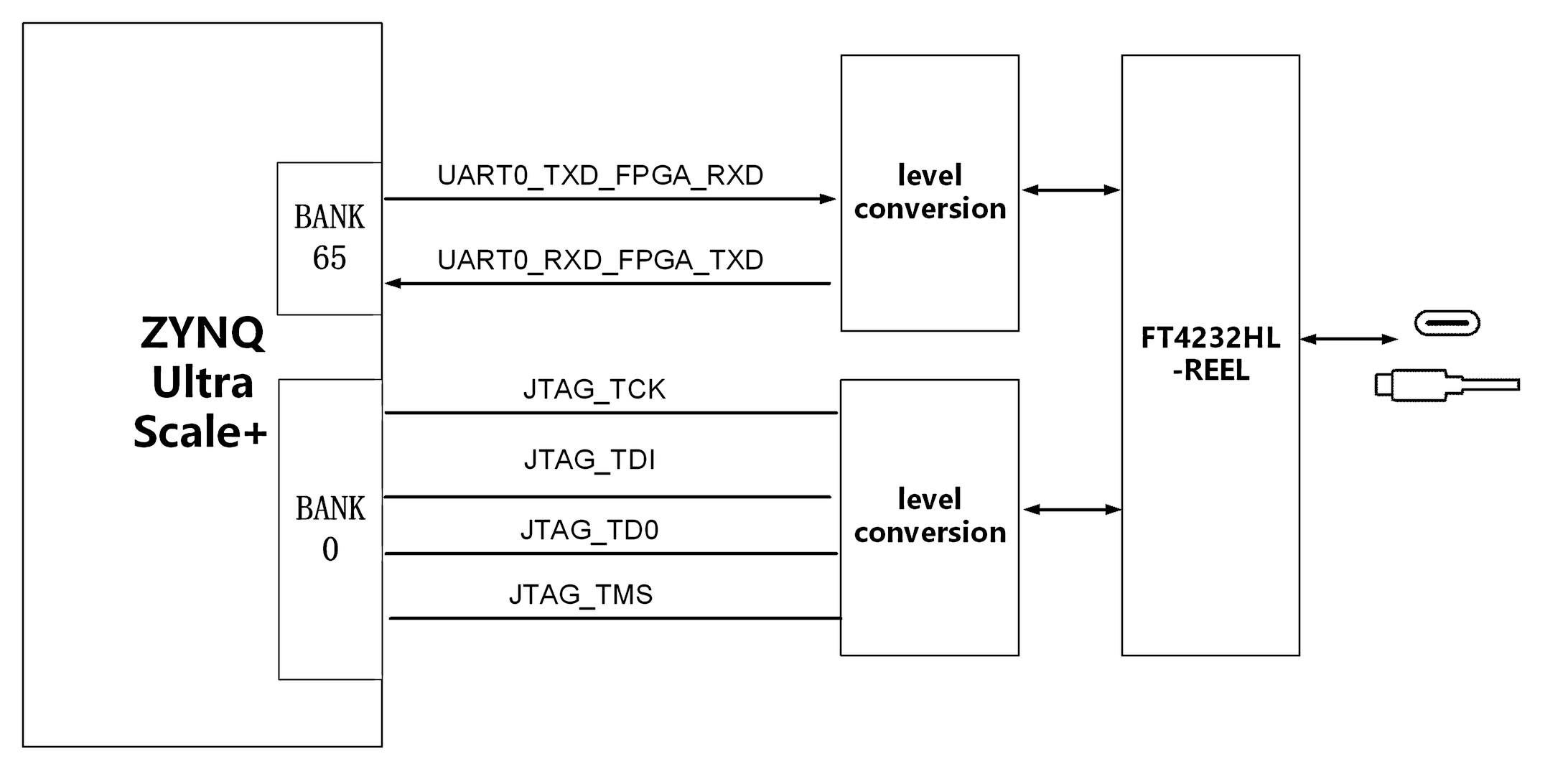
Figure 4.8.2 - Schematic diagram of JTAG & UART connector connection on the KU115 side.
| Signal name | pin name | pin number | Remark |
| UART0_TXD_FPGA_RXD | IO_L23P_T3U_N8_I2C_SCLK_65_AM27 | AM27 | UART data output |
| UART0_RXD_FPGA_TXD | IO_L20P_T3L_N2_AD1P_D08_65_AN28 | AN28 | UART data input |
Table 4.8.2 - KU115 Side JTAG & UART Pin Assignment
4.9 DDR4 memory
The carrier board is equipped with 16 Micron 1GB DDR4 chips, model MT40A512M16LY-075:E . Specifically, 4 DDR4 chips are mounted on BANK44, 45, and 46 of the KU115 module ; 4 on BANK66, 67, and 68 ; 4 on BANK51 , 52, and 53; and 4 on BANK71, 72, and 73 , forming a 64- bit data bus bandwidth. The maximum operating speed of the DDR4 SDRAM can reach 1200MHz (data rate 2400Mbps). The specific configuration of the DDR4 SDRAM is shown in the table below .
| Location | Position | Chip Model | capacity | factory |
| KU115 | M1~M16 | MT40A512M16LY-075:E | 512x16bit | Micron |
Table 4.9.1 - DDR4 Models and Specifications
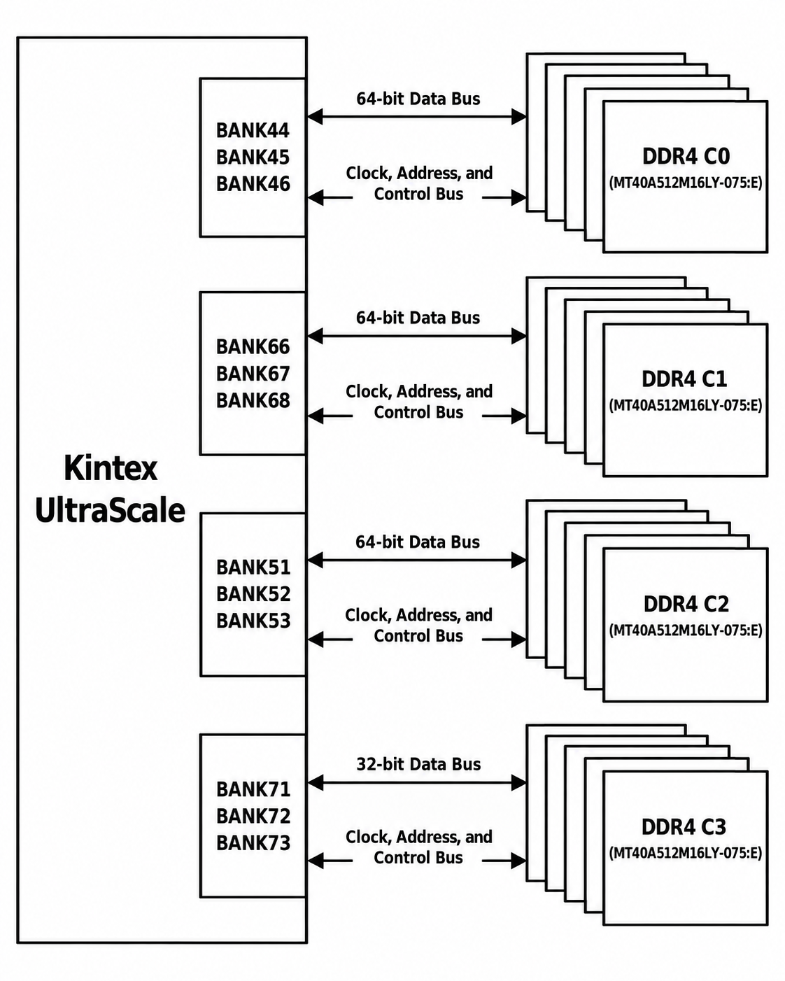
Figure 4.9.1 - DDR4 SDRAM Connection Diagram
4.10 QSPI Flash
The carrier board is equipped with two 512Mbit FLASH chips forming an 8-bit bandwidth data bus. The FLASH model is MT25QU512AB , and it operates at 1.8V. Due to the non-volatile nature of QSPI FLASH, it can be used as a system boot device to store the system boot image. These images mainly include the FPGA bit file, the ARM application code, and its user data file. Specific QSPI FLASH models and related characteristics are shown in the table below .
| Location | Position | Chip Model | capacity | factory |
| KU115 BANK65 | U7, U8 | MT25QU512AB | 512Mb | Micron |
Table 4.10.1 - QSPI FLASH Models and Parameters
The QSPI FLASH is connected to the BANK 65 of the KU115 chip .
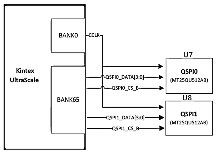
Figure 4.10.1 - Schematic diagram of QSPI FLASH connection on KU115
| FPGA (U1) pin names | signal name | QSPI pin numbers | QSPI pin names |
| CCLK_0_AG13 | FPGA_CCLK | U7.B2 | C_B2 |
| D02_0_AL12 | SPI0_WP# | U7.C4 | W#DQ2 |
| D01_DIN_0_AJ12 | SPI0_DQ1 | U7.D2 | DQ1 |
| D00_MOSI_0_AK12 | SPI0_DQ0 | U7.D3 | DQ0 |
| D03_0_AH12 | SPI0_HOLD_B | U7.D4 | DQ3_H0LD_B |
| RDWR_FCS_B_0_AG12 | SPI0_CS_B | U7.C2 | S# |
| IO_L2N_T0L_N3_FWE_FCS2_B_65_BF27 | SPI1_CS_B | U8.C2 | S# |
| IO_L22P_T3U_N6_DBC_AD0P_D04_65_AM26 | SPI1_DQ0 | U8.D3 | DQ0 |
| IO_L21N_T3L_N5_AD8N_D07_65_AM25 | SPI1_HOLD_B | U8.D4 | DQ3_HOLD_B |
| IO_L21P_T3L_N4_AD8P_D06_65_AL25 | SPI1_WP | U8.C4 | W#DQ2 |
| IO_L22N_T3U_N7_DBC_AD0N_D05_65_AN26 | SPI1_DQ1 | U8.D2 | DQ1 |
| CCLK_0_AG13 | FPGA_CCLK | U8.B2 | C_B2 |
Table 4.10.2 - Pin Assignment of QSPI FLASH Chip on KU115
4.11 Fiber Optic Interface
The carrier board has three fiber optic interfaces: one SFP interface and two QSFP interfaces. These three fiber optic interfaces connect to the GT transceivers on the KU115 's BANK226, BANK230 , and BANK231 , respectively. The GT BANK's reference clock can be provided by a 156.25MHz differential crystal oscillator on the carrier board or by a 156.25MHz Si5341 . A schematic diagram of the fiber optic interface connections is shown below:
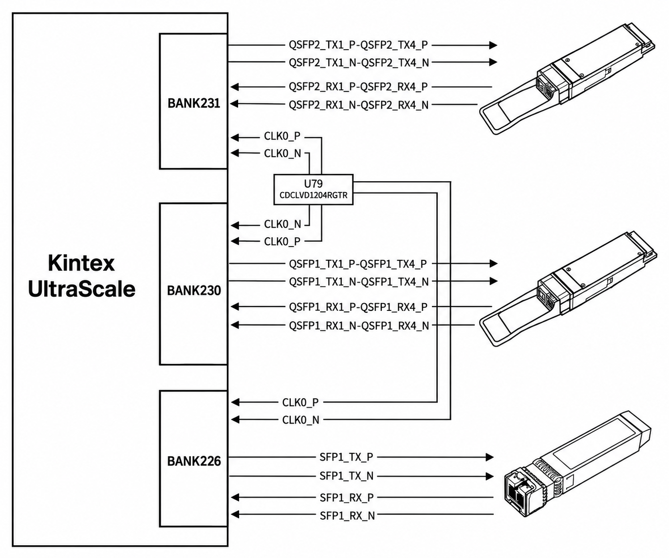
Figure 4.11.1 - Schematic diagram of fiber optic design
| Signal name | ZYNQ pin name | ZYNQ pin number |
| QSFP1_TX1_P | MGTHTXP0_230_U9 | U9 |
| QSFP1_TX1_N | MGTHTXN0_230_U8 | U8 |
| QSFP1_RX1_P | MGTHRXP0_230_U4 | U4 |
| QSFP1_RX1_N | MGTHRXN0_230_U3 | U3 |
| QSFP1_TX2_P | MGTHTXP1_230_T7 | T7 |
| QSFP1_TX2_N | MGTHTXN1_230_T6 | T6 |
| QSFP1_RX2_P | MGTHRXP1_230_T2 | T2 |
| QSFP1_RX2_N | MGTHRXN1_230_T1 | T1 |
| QSFP1_TX3_P | MGTHTXP2_230_R9 | R9 |
| QSFP1_TX3_N | MGTHTXN2_230_R8 | R8 |
| QSFP1_RX3_P | MGTHRXP2_230_R4 | R4 |
| QSFP1_RX3_N | MGTHRXN2_230_R3 | R3 |
| QSFP1_TX4_P | MGTHTXP3_230_P7 | P7 |
| QSFP1_TX4_N | MGTHTXN3_230_P6 | P6 |
| QSFP1_RX4_P | MGTHRXP3_230_P2 | P2 |
| QSFP1_RX4_N | MGTHRXN3_230_P1 | P1 |
| QSFP2_TX1_P | MGTHTXP0_231_N9 | N9 |
| QSFP2_TX1_N | MGTHTXN0_231_N8 | N8 |
| QSFP2_RX1_P | MGTHRXP0_231_N4 | N4 |
| QSFP2_RX1_N | MGTHRXN0_231_N3 | N3 |
| QSFP2_TX2_P | MGTHTXP1_231_M7 | M7 |
| QSFP2_TX2_N | MGTHTXN1_231_M6 | M6 |
| QSFP2_RX2_P | MGTHRXP1_231_M2 | M2 |
| QSFP2_RX2_N | MGTHRXN1_231_M1 | M1 |
| QSFP2_TX3_P | MGTHTXP2_231_L9 | L9 |
| QSFP2_TX3_N | MGTHTXN2_231_L8 | L8 |
| QSFP2_RX3_P | MGTHRXP2_231_L4 | L4 |
| QSFP2_RX3_N | MGTHRXN2_231_L3 | L3 |
| QSFP2_TX4_P | MGTHTXP3_231_K7 | K7 |
| QSFP2_TX4_N | MGTHTXN3_231_K6 | K6 |
| QSFP2_RX4_P | MGTHRXP3_231_K2 | K2 |
| QSFP2_RX4_N | MGTHRXN3_231_K1 | K1 |
Table 4.11.1 - QSFP Interface Pin Assignment
| Signal name | ZYNQ pin name | ZYNQ pin number | Remark |
| GT230_REFCLK0_C_P | MGTREFCLK0P_230_T11 | T11 | The OUT3 output of the CDCLVD1204RGTR is configured with a 156.25MHz crystal oscillator by default, and can be optionally output from a Si5341. |
| GT230_REFCLK0_C_N | MGTREFCLK0N_230_T10 | T10 | The OUT3 output of the CDCLVD1204RGTR is configured with a 156.25MHz crystal oscillator by default, and can be optionally output from a Si5341. |
| MGB1_REFCLK1_P | MGTREFCLK1P_230_P11 | P11 | Connector ARF6-16-SDAK-TR output |
| MGB1_REFCLK1_N | MGTREFCLK1N_230_P10 | P10 | Connector ARF6-16-SDAK-TR output |
| GT231_REFCLK0_C_P | MGTREFCLK0P_231_M11 | M11 | The OUT2 output of the CDCLVD1204RGTR is configured with a 156.25MHz crystal oscillator by default, and can be optionally output from a Si5341. |
| GT231_REFCLK0_C_N | MGTREFCLK0N_231_M10 | M10 | The OUT2 output of the CDCLVD1204RGTR is configured with a 156.25MHz crystal oscillator by default, and can be optionally output from a Si5341. |
| GT226_REFCLK0_C_P | MGTREFCLK0P_226_AM11 | AM11 | The OUT1 output of the CDCLVD1204RGTR is configured with a 156.25MHz crystal oscillator by default, and can be optionally output from a Si5341. |
| GT226_REFCLK0_C_N | MGTREFCLK0N_226_AM10 | AM10 | The OUT1 output of the CDCLVD1204RGTR is configured with a 156.25MHz crystal oscillator by default, and can be optionally output from a Si5341. |
Table 4.11.2 - Reference Clock Allocation for BANK230, BANK231, and BANK226
| Signal name | ZYNQ pin name | ZYNQ pin number |
| SFP1_RX_P | MGTHRXP3_226_AK2 | AK2 |
| SFP1_RX_N | MGTHRXN3_226_AK1 | AK1 |
| SFP1_TX_P | MGTHTXP3_226_AK7 | AK7 |
| SFP1_TX_N | MGTHTXN3_226_AK6 | AK6 |
Table 4.11.3 - SFP Interface Pin Assignment
Low-speed control I/O processing:
| QSFP low-speed IO signal name | Remark | SFP low-speed IO signal name | Remark |
| MODSELL | pull down GND | txfault_0 | 3.3V pull-up |
| ResetL | 3.3V pull-up | mod_def0_0 | 3.3V pull-up |
| MODPRSL | 3.3V pull-up | mod_def1_0 | 3.3V pull-up |
| SDA | 3.3V pull-up | mod_def2_0 | 3.3V pull-up |
| SCL | 3.3V pull-up | los_0 | 3.3V pull-up |
| intL | 3.3V pull-up | txdisable_0 | pull down GND |
| LPMode | pull down GND | ||
Table 4.11.4 - Fiber Optic Low-Speed I/O Signal Processing Method
4.12 M.2 Interface
The carrier board features four PCIe x 4 standard M.2 interfaces for connecting M.2 SSDs. The M.2 interfaces use M-key slots and only support PCIe, not SATA. Users must select a PCIe type SSD. The PCIe signals are directly connected to BANK227, BANK228, BANK232, and BANK233 of the KU115 . The TX and RX signals are differentially connected to LANE0, LANE1 , LANE2 , and LANE3 of the MGT . The PCIe clock is provided by a 100MHz differential clock . The M.2 circuit design diagram is shown below:
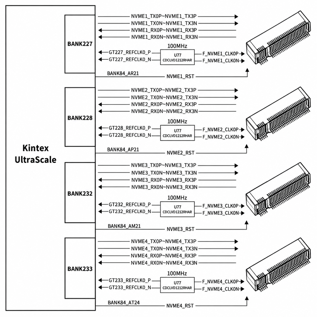
Figure 4.12.1 - NVMe Interface Design Diagram
| Signal name | FPGA pin names | NVMe connector | |
| pin number | name | ||
| F_NVME1_TX0P | MGTHTXP3_227_AF7 | U18.49 | PERP0 |
| F_NVME1_TX0N | MGTHTXN3_227_AF6 | U18.47 | PERN0 |
| F_NVME1_RX0P | MGTHRXP3_227_AF2 | U18.43 | PETP0 |
| F_NVME1_RX0N | MGTHRXN3_227_AF1 | U18.41 | PETN0 |
| F_NVME1_TX1P | MGTHTXP2_227_AG9 | U18.37 | PERP1 |
| F_NVME1_TX1N | MGTHTXN2_227_AG8 | U18.35 | PERN1 |
| F_NVME1_RX1P | MGTHRXP2_227_AG4 | U18.31 | PETP1 |
| F_NVME1_RX1N | MGTHRXN2_227_AG3 | U18.29 | PETN1 |
| F_NVME1_TX2P | MGTHTXP1_227_AH7 | U18.25 | PERP2 |
| F_NVME1_TX2N | MGTHTXN1_227_AH6 | U18.23 | PERN2 |
| F_NVME1_RX2P | MGTHRXP1_227_AH2 | U18.19 | PETP2 |
| F_NVME1_RX2N | MGTHRXN1_227_AH1 | U18.17 | PETN2 |
| F_NVME1_TX3P | MGTHTXP0_227_AJ9 | U18.13 | PERP3 |
| F_NVME1_TX3N | MGTHTXN0_227_AJ8 | U18.11 | PERN3 |
| F_NVME1_RX3P | MGTHRXP0_227_AJ4 | U18.7 | PETP3 |
| F_NVME1_RX3N | MGTHRXN0_227_AJ3 | U18.5 | PETN3 |
| GT227_REFCLK0_P | MGTREFCLK0P_227_AH11 | ||
| GT227_REFCLK0_N | MGTREFCLK0N_227_AH10 | ||
| F_NVME2_TX0P | MGTHTXP3_228_AB7 | U19.49 | PERP0 |
| F_NVME2_TX0N | MGTHTXN3_228_AB6 | U19.47 | PERN0 |
| F_NVME2_RX0P | MGTHRXP3_228_AB2 | U19.43 | PETP0 |
| F_NVME2_RX0N | MGTHRXN3_228_AB1 | U19.41 | PETN0 |
| F_NVME2_TX1P | MGTHTXP2_228_AC9 | U19.37 | PERP1 |
| F_NVME2_TX1N | MGTHTXN2_228_AC8 | U19.35 | PERN1 |
| F_NVME2_RX1P | MGTHRXP2_228_AC4 | U19.31 | PETP1 |
| F_NVME2_RX1N | MGTHRXN2_228_AC3 | U19.29 | PETN1 |
| F_NVME2_TX2P | MGTHTXP1_228_AD7 | U19.25 | PERP2 |
| F_NVME2_TX2N | MGTHTXN1_228_AD6 | U19.23 | PERN2 |
| F_NVME2_RX2P | MGTHRXP1_228_AD2 | U19.19 | PETP2 |
| F_NVME2_RX2N | MGTHRXN1_228_AD1 | U19.17 | PETN2 |
| F_NVME2_TX3P | MGTHTXP0_228_AE9 | U19.13 | PERP3 |
| F_NVME2_TX3N | MGTHTXN0_228_AE8 | U19.11 | PERN3 |
| F_NVME2_RX3P | MGTHRXP0_228_AE4 | U19.7 | PETP3 |
| F_NVME2_RX3N | MGTHRXP0_228_AE 3 | U19.5 | PETN3 |
| GT228_REFCLK0_P | MGTREFCLK0P_228_AD11 | ||
| GT228_REFCLK0_N | MGTREFCLK0N_228_AD10 | ||
| F_NVME3_TX0P | MGTHTXP3_232_F7 | U20.49 | PERP0 |
| F_NVME3_TX0N | MGTHTXN3_232_F6 | U20.47 | PERN0 |
| F_NVME3_RX0P | MGTHRXP3_232_F2 | U20.43 | PETP0 |
| F_NVME3_RX0N | MGTHRXN3_232_F1 | U20.41 | PETN0 |
| F_NVME3_TX1P | MGTHTXP2_232_G9 | U20.37 | PERP1 |
| F_NVME3_TX1N | MGTHTXN2_232_G8 | U20.35 | PERN1 |
| F_NVME3_RX1P | MGTHRXP2_232_G4 | U20.31 | PETP1 |
| F_NVME3_RX1N | MGTHRXN2_232_G3 | U20.29 | PETN1 |
| F_NVME3_TX2P | MGTHTXP1_232_H7 | U20.25 | PERP2 |
| F_NVME3_TX2N | MGTHTXN1_232_H6 | U20.23 | PERN2 |
| F_NVME3_RX2P | MGTHRXP1_232_H2 | U20.19 | PETP2 |
| F_NVME3_RX2N | MGTHRXN1_232_H1 | U20.17 | PETN2 |
| F_NVME3_TX3P | MGTHTXP0_232_J9 | U20.13 | PERP3 |
| F_NVME3_TX3N | MGTHTXN0_232_J8 | U20.11 | PERN3 |
| F_NVME3_RX3P | MGTHRXP0_232_J4 | U20.7 | PETP3 |
| F_NVME3_RX3N | MGTHRXN0_232_J3 | U20.5 | PETN3 |
| GT232_REFCLK0_P | MGTREFCLK0P_232_H11 | ||
| GT232_REFCLK0_N | MGTREFCLK0N_232_H10 | ||
| F_NVME4_TX0P | MGTHTXP3_233_A9 | U21.49 | PERP0 |
| F_NVME4_TX0N | MGTHTXN3_233_A8 | U21.47 | PERN0 |
| F_NVME4_RX0P | MGTHRXP3_233_A5 | U21.43 | PETP0 |
| F_NVME4_RX0N | MGTHRXN3_233_A4 | U21.41 | PETN0 |
| F_NVME4_TX1P | MGTHTXP2_233_C9 | U21.37 | PERP1 |
| F_NVME4_TX1N | MGTHTXN2_233_C8 | U21.35 | PERN1 |
| F_NVME4_RX1P | MGTHRXP2_233_C4 | U21.31 | PETP1 |
| F_NVME4_RX1N | MGTHRXN2_233_C3 | U21.29 | PETN1 |
| F_NVME4_TX2P | MGTHTXP1_233_D7 | U21.25 | PERP2 |
| F_NVME4_TX2N | MGTHTXN1_233_D6 | U21.23 | PERN2 |
| F_NVME4_RX2P | MGTHRXP1_233_D2 | U21.19 | PETP2 |
| F_NVME4_RX2N | MGTHRXN1_233_D1 | U21.17 | PETN2 |
| F_NVME4_TX3P | MGTHTXP0_233_E9 | U21.13 | PERP3 |
| F_NVME4_TX3N | MGTHTXN0_233_E8 | U21.11 | PERN3 |
| F_NVME4_RX3P | MGTHRXP0_233_E4 | U21.7 | PETP3 |
| F_NVME4_RX3N | MGTHRXN0_233_E3 | U21.5 | PETN3 |
| GT233_REFCLK0_P | MGTREFCLK0P_233_D11 | ||
| GT233_REFCLK0_N | MGTREFCLK0N_233_D10 | ||
Table 4.12.1 - NVMe Interface KU115 Pin Assignment
4.13 Expand MGB Interface
The expansion board has two MGB interfaces, which can expand to two PCIe x 4 interfaces, supporting the PCIe Gen3.0 protocol. Four pairs of transceivers connect to the connector (ARF6-16-SDAK-TR) for data communication. The interface's transmit and receive signals are directly connected to the FPGA BANK229 and BANK224 transceivers. All four TX and RX signals are connected to the FPGA transceivers in a differential signal configuration .
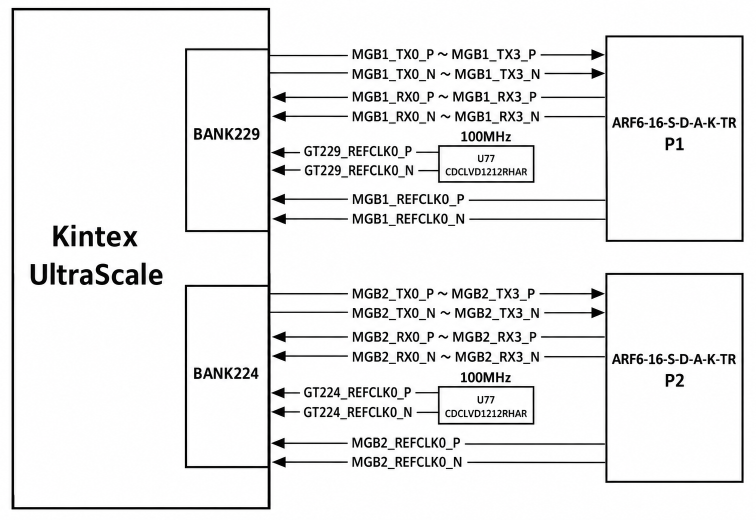
Figure 4.13.1 - Schematic diagram of MGB interface design
| Signal name | FPGA pin names | MGB connector | |
| pin number | name | ||
| MGB1_RX0_P | MGTHRXP0_229_AA4 | 03 | RX0_P |
| MGB1_RX0_N | MGTHRXN0_229_AA3 | 05 | RX0_N |
| MGB1_RX1_P | MGTHRXP1_229_Y2 | 09 | RX1_P |
| MGB1_RX1_N | MGTHRXN1_229_Y1 | 11 | RX1_N |
| MGB1_RX2_P | MGTHRXP2_229_W4 | 15 | RX2_P |
| MGB1_RX2_N | MGTHRXN2_229_W3 | 17 | RX2_N |
| MGB1_RX3_P | MGTHRXP3_229_V2 | 21 | RX3_P |
| MGB1_RX3_N | MGTHRXN3_229_V1 | 23 | RX3_N |
| MGB1_TX0_P | MGTHTXP0_229_AA9 | 04 | TX0_P |
| MGB1_TX0_N | MGTHTXN0_229_AA8 | 06 | TX0_N |
| MGB1_TX1_P | MGTHTXP1_229_Y7 | 10 | TX1_P |
| MGB1_TX1_N | MGTHTXN1_229_Y6 | 12 | TX1_N |
| MGB1_TX2_P | MGTHTXP2_229_W9 | 16 | TX2_P |
| MGB1_TX2_N | MGTHTXN2_229_W8 | 18 | TX2_N |
| MGB1_TX3_P | MGTHTXP3_229_V7 | 22 | TX3_P |
| MGB1_TX3_N | MGTHTXN3_229_V6 | 24 | TX3_N |
| MGB1_REFCLK1_P | MGTREFCLK1P_230_P11 | 27 | REFCLK1_P |
| MGB1_REFCLK1_N | MGTREFCLK1N_230_P10 | 29 | REFCLK1_N |
| MGB1_REFCLK0_P | MGTREFCLK1P_229_V11 | 38 | REFCLK0_P |
| MGB1_REFCLK0_N | MGTREFCLK1N_229_V10 | 30 | REFCLK0_N |
| MGB2_RX0_P | MGTHRXP0_224_BC2 | 03 | RX0_P |
| MGB2_RX0_N | MGTHRXN0_224_BC1 | 05 | RX0_N |
| MGB2_RX1_P | MGTHRXP1_224_BA2 | 09 | RX1_P |
| MGB2_RX1_N | MGTHRXN1_224_BA1 | 11 | RX1_N |
| MGB2_RX2_P | MGTHRXP2_224_AW4 | 15 | RX2_P |
| MGB2_RX2_N | MGTHRXN2_224_AW3 | 17 | RX2_N |
| MGB2_RX3_P | MGTHRXP3_224_AV2 | 21 | RX3_P |
| MGB2_RX3_N | MGTHRXN3_224_AV1 | 23 | RX3_N |
| MGB2_TX0_P | MGTHTXP0_224_BF5 | 04 | TX0_P |
| MGB2_TX0_N | MGTHTXN0_224_BF4 | 06 | TX0_N |
| MGB2_TX1_P | MGTHTXP1_224_BD5 | 10 | TX1_P |
| MGB2_TX1_N | MGTHTXN1_224_BD4 | 12 | TX1_N |
| MGB2_TX2_P | MGTHTXP2_224_BB5 | 16 | TX2_P |
| MGB2_TX2_N | MGTHTXN2_224_BB4 | 18 | TX2_N |
| MGB2_TX3_P | MGTHTXP3_224_AV7 | 22 | TX3_P |
| MGB2_TX3_N | MGTHTXN3_224_AV6 | 24 | TX3_N |
| MGB2_REFCLK1_P | MGTREFCLK1P_225_AP11 | 27 | REFCLK1_P |
| MGB2_REFCLK1_N | MGTREFCLK1N_225_AP10 | 29 | REFCLK1_N |
| MGB2_REFCLK0_P | MGTREFCLK1P_224_AV11 | 38 | REFCLK0_P |
| MGB2_REFCLK0_N | MGTREFCLK1N_224_AV10 | 30 | REFCLK0_N |
Table 4.13.1 - MGB Interface Pin Assignment
4.14 Expand I/O , LEDs , and Buttons
The carrier board has two sets of I/O (X4) extended on the RFSoC side.
J11 Extended I/O Pin Assignment:
| Signal name | ZYNQ pin name | ZYNQ pin number |
| IO_L2P | IO_L2P_T0L_N2_66_AP6 | AP6 |
| IO_L2N | IO_L1N_T0L_N1_DBC_66_AP7 | AP7 |
| IO_L1P | IO_L1P_T0L_N0_DBC_66_AP8 | AP8 |
| IO_L1N | IO_L4P_T0U_N6_DBC_AD7P_66_AN5 | AN5 |
Table 4.14.1 - PL Side J11 Side Extended IO Pin Assignment
J12 Side Expansion I/O Pin Assignment
| Signal name | ZYNQ pin name | ZYNQ pin number |
| BANK501_MIO40 | PS_MIO40_A18 | A18 |
| BANK500_MIO24 | PS_MIO24_A17 | A17 |
| BANK501_MIO44 | PS_MIO44_C20 | C20 |
| BANK500_MIO6 | PS_MIO6_H16 | H16 |
Table 4.14.2 - PS Side J12 Expansion I/O Pin Assignment
Four user-customizable LEDs are extended on the RFSoC side of the carrier board, and four IOs are connected to the LEDs . The pin assignments are shown in the table below.
| Signal name | ZYNQ pin name | ZYNQ pin number |
| LED0 | IO_T3U_N12_66_AH12 | AH12 |
| LED1 | IO_L6N_T0U_N11_AD6N_66_AN1 | AN1 |
| LED2 | IO_L6P_T0U_N10_AD6P_66_AN2 | AN2 |
| LED3 | IO_L2N_T0L_N3_66_AP5 | AP5 |
Table 4.14.3 - RFSoC Side LED Expansion IO Pin Assignment
Eight user-customizable LEDs are extended from the KU115 side of the carrier board, and eight I/O pins are routed to the LEDs.
| Signal name | ZYNQ pin name | ZYNQ pin number |
| User_LED_0 | IO_L2P_T0L_N2_FOE_B_65_BE27 | BE27 |
| User_LED_1 | IO_L1P_T0L_N0_DBC_RS0_65_BF28 | BF28 |
| User_LED_2 | IO_L4N_T0U_N7_DBC_AD7N_A25_65_BE26 | BE26 |
| User_LED_3 | IO_L6N_T0U_N11_AD6N_A21_65_BC27 | BC27 |
| User_LED_4 | IO_L3N_T0L_N5_AD15N_A27_65_BE28 | BE28 |
| User_LED_5 | IO_L4P_T0U_N6_DBC_AD7P_A24_65_BD26 | BD26 |
| User_LED_6 | IO_T0U_N12_A28_65_BD25 | BD25 |
| User_LED_7 | IO_L1N_T0L_N1_DBC_RS1_65_BF29 | BF29 |
Table 4.14.4 - KU115 Side LED Expansion IO Pin Assignment
Five user-customizable buttons and five IO ports are extended on the RFSoC side of the carrier board, and a KU115 SW2 is added.
| Signal name | ZYNQ pin name | ZYNQ pin number |
| BANK88_IO_L10P | IO_L10P_AD10P_88_C14 | C14 |
| BANK88_IO_L10N | IO_L10N_AD10N_88_B13 | B13 |
| BANK88_IO_L11P | IO_L11P_AD9P_88_A14 | A14 |
| BANK88_IO_L11N | IO_L11N_AD9N_88_A13 | A13 |
| IO_L4N_T0U_N7_DBC_AD7N_66_AN4_1V2 | IO_L4N_T0U_N7_DBC_AD7N_66_AN4 | AN4 |
Table 4.14.5 - RFSoC Side Button Expansion I/O Pin Assignment
| Signal name | ZYNQ pin name | ZYNQ pin number |
| USER_SW_DP0 | IO_L18P_T2U_N10_AD2P_D12_65_AR28 | AR28 |
| USER_SW_DP1 | IO_L15N_T2L_N5_AD11N_A03_D19_65_AU27 | AU27 |
| USER_SW_DP2 | IO_L14N_T2L_N3_GC_A05_D21_65_AV28 | AV28 |
| USER_SW_DP3 | IO_L14P_T2L_N2_GC_A04_D20_65_AV27 | AV27 |
Table 4.14.6 - KU115 Side SW Expansion IO Pin Assignment
4.15 Power Supply
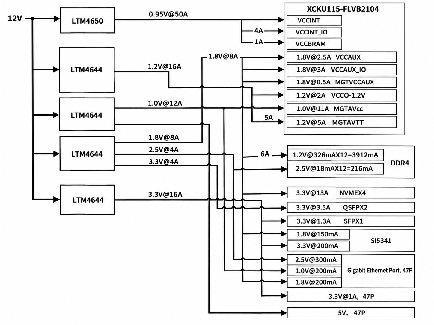
The carrier board's power input voltage is VCC12_SW , and the carrier board generates multiple power supplies such as +5V, + 1.8V, and +3.3V through a multi-channel power chip . The power supply design block diagram can be found in the schematic .
4.16 Structural Dimensions Drawing
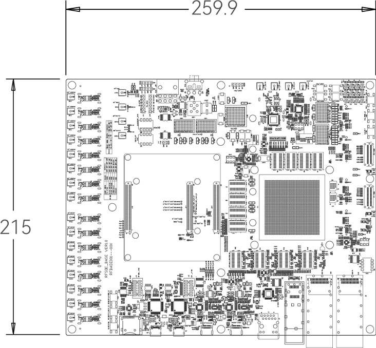
Figure 4.16.1 - Front view of the base plate structure
Appendix: List of Abbreviations
Contact information
Alinx Electronic Limited
Company Website: www.en.alinx.com
Service Hotline: +86 21 67676997
Technical Support:technical@alinx.com