
Appearance
BZ11 User Manual

Alinx Electronic Limited
Company Website: www.en.alinx.com
Service Hotline: +86 21 67676997
Technical Support: technical@alinx.com
Document Information
| Item | Content |
| Document Name | User Manual |
| Product Model | BZ11 |
| Document Version | V1.0 |
| Prepared by | Alinx Electronic Limited |
| Release Date | 2026.11.9 |
Document Revision History
| Version | Date | Section | Revision Summary |
| V1.0 | 2026.11.9 | All | Initial Release |
Overview
Alinx Electronic Limited has officially released the 2025 model of its development board (Model: BZ11) based on the Xilinx Zynq UltraScale+ MPSoC development platform. To help you quickly understand this development platform, we have prepared this user manual.
This MPSoC development platform adopts the Xilinx Zynq UltraScale+ MPSoCs series chip, model XCZU11EG-2FFVC1156I, as its main chip. The ZU11EG chip can be divided into a Processor System (PS) and a Programmable Logic (PL). In addition, the PS side of the FPGA on the development board carries four high-speed DDR4 SDRAM chips with a total of 4GB, one 32GB eMMC storage chip and two 256Mbit QSPI FLASH chips. In the carrier board design we have expanded abundant peripheral interfaces for users, such as 4 FMC HPC connectors, one M.2 SSD interface, one mini_DP interface, one USB3.0 Type-C interface, one Gigabit Ethernet interface, one UART interface, one QSFP+ fiber optic interface and one TF card interface. This development board can meet the requirements of high-speed data exchange, data storage and video transmission processing. It is suitable for AI, edge computing, deep learning, data centers, medical imaging, multimedia, 4K video images, digital signal processing, machine vision, 5G wireless, aerospace radar and satellites, automotive ADAS, in-vehicle simulation and testing, semiconductor simulation and design, and industrial IoT.
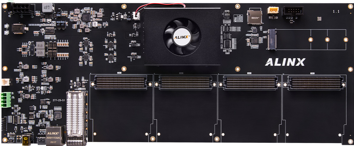
Figure 1.1 - BZ11 Development Board
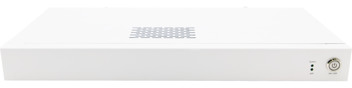
Figure 1.2 - BZ11 Computing Box
The following figure shows the structure of the entire development system:
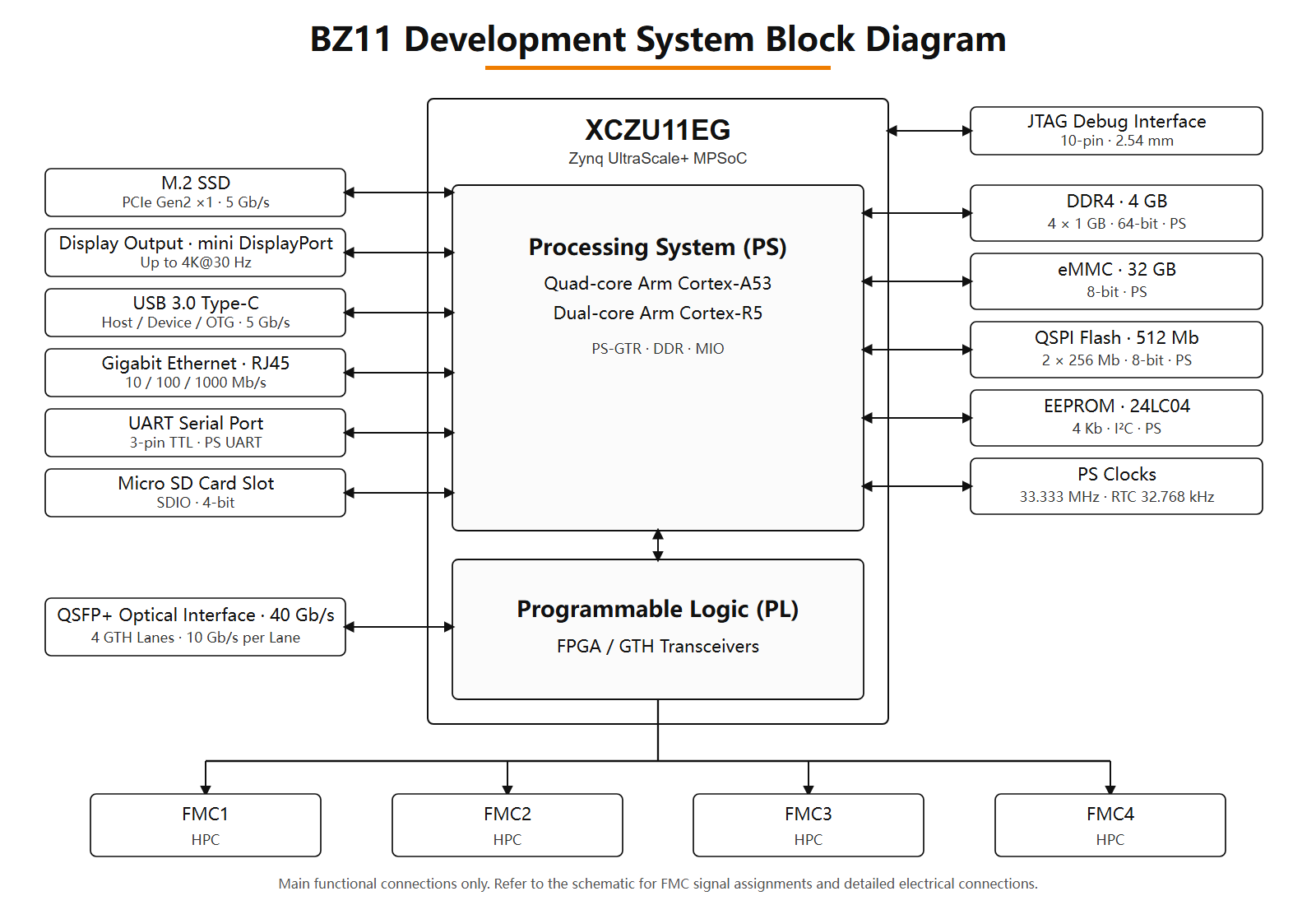
Figure 1.3 - Development System Structure Diagram
From this figure, we can see the interfaces and functions provided by this development platform.
ZU11EG: composed of ZU11EG + 4GB DDR4 (PS) + 32GB eMMC FLASH + 64MB QSPI FLASH.
M.2 Interface: one standard PCIe Gen2 x1 M.2 interface for connecting M.2 SSDs, with a single-lane communication speed of up to 5Gbps.
DP Output Interface: one standard DisplayPort output interface for video image display, supporting up to 4K@30Hz or 1080P@60Hz output.
USB 3.0 Interface: one USB 3.0 interface with a Type-C connector, supporting HOST, SLAVE and OTG modes.
Gigabit Ethernet Interface: one 10/100/1000 Mbps Ethernet RJ45 interface on the PS side for Ethernet data exchange with a PC or other network devices.
QSFP+ Fiber Optic Interface: four high-speed GTH transceivers of the FPGA are connected to one QSFP+ optical module interface to implement a QSFP+ fiber optic communication interface, with fiber data transmission and reception speeds of up to 40Gbps.
Micro SD Card Socket: one Micro SD card socket for storing the operating system image and file system.
FMC Expansion Connectors: four standard FMC HPC expansion connectors, which can be connected to various FMC modules from Xilinx or ALINX (HDMI input/output module, GMSL video capture module, GMSL video injection module, etc.).
JTAG Debug Port: one 10-pin 2.54mm standard JTAG interface for FPGA program download and debugging; users can debug and download the ZU11EG system with a Xilinx downloader.
EEPROM: one EEPROM 24LC04 with an I2C interface.
LEDs: four light-emitting diodes (LEDs) and one dual-layer LED. The board has one power indicator, one DONE configuration indicator and two user indicators; the dual-layer LED is connected to the PS side.
Push Button: one side-mounted reset button.
Zynq Chip
The development board uses the Xilinx Zynq UltraScale+ MPSoC series chip, model XCZU11EG-2FFVC1156I. The PS of the ZU11EG integrates a quad-core ARM Cortex-A53 processor running at up to 1.3GHz with L2 cache support; the ZU11EG also includes a dual-core Cortex-R5 processor running at up to 533MHz.
The ZU11EG supports 32-bit or 64-bit DDR4, LPDDR4, DDR3, DDR3L and LPDDR3 memory chips, and provides rich high-speed interfaces on the PS side such as PCIe Gen2, USB 3.0, SATA 3.1 and DisplayPort, as well as USB 2.0, Gigabit Ethernet, SD/SDIO, I2C, CAN, UART and GPIO. The PL contains abundant programmable logic cells, DSP slices and internal RAM. The overall block diagram of the ZU11EG chip is shown in Figure 2.1.
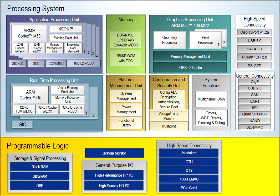
Figure 2.1 - ZYNQ ZU11EG Chip Overall Block Diagram
The main parameters of the PS are as follows:
ARM quad-core Cortex-A53 processor at up to 1.3GHz, with 32KB L1 instruction and data cache per CPU and a 1MB L2 cache shared by the two CPUs.
ARM dual-core Cortex-R5 processor at up to 533MHz, with 32KB L1 instruction and data cache per CPU and 128KB tightly coupled memory.
Mali-400 MP2 image/video processor at up to 677MHz with 64KB L2 cache.
External memory interface, supporting 32/64-bit DDR4/3/3L, LPDDR4/3, etc.
Static memory interface, supporting NAND and 2x Quad-SPI FLASH.
High-speed connectivity: PCIe Gen2 x4, 2x USB3.0, SATA 3.1, DisplayPort and 4x Tri-mode Gigabit Ethernet.
General connectivity: 2x USB2.0, 2x SD/SDIO, 2x UART, 2x CAN 2.0B, 2x I2C, 2x SPI and 4x 32b GPIO.
Power management: supports the Full, Low, PL and Battery power domains.
Encryption: supports RSA, AES and SHA.
System monitor: 10-bit 1Mbps AD sampling for temperature and voltage monitoring.
The main parameters of the PL are as follows:
System Logic Cells: 653.1K;
CLB flip-flops: 597.12K;
CLB LUTs: 298.56K;
Block RAM: 21.1Mb;
Clock Management Tiles (CMTs): 8
DSP Slices: 2928
GTH 16.3Gb/s transceivers: 20
The speed grade of the XCZU11EG-2FFVC1156I chip is -2, industrial grade, in an FFVC1156 package.
DDR4
The BZ11 board is equipped with four 1GB Micron DDR4 chips, model MT40A512M16LY-062E. Four DDR4 chips are mounted on the PS side, forming a 64-bit data bus width and 4GB capacity. The PS-side DDR4 SDRAM runs at up to 1200MHz (2400Mbps data rate), and the four DDR4 memory chips are connected directly to the memory interface of PS BANK504. The specific configuration of the PS-side DDR4 SDRAM is shown in Table 3.1.
| Position | Ref. Designator | Part Number | Capacity | Manufacturer |
| PS | U4、U5、U6、U7 | MT40A512M16LY-062E | 512M x 16bit | Micron |
Table 3.1 - DDR4 SDRAM Configuration
DDR4 hardware design requires strict consideration of signal integrity. We have fully considered matching resistors, termination resistors, trace impedance control and trace length matching in the circuit and PCB design to ensure stable high-speed operation of DDR4.
The hardware connection of the PS-side DDR4 is shown in Figure 3.1:
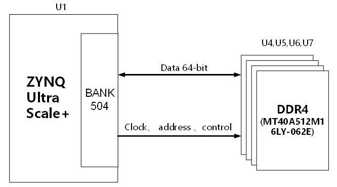
Figure 3.1 - PS-Side DDR4 DRAM Schematic
PS-Side DDR4 SDRAM Pin Assignment:
| Signal Name | Pin Name | Pin Number |
| PS_DDR4_DQS0_N | PS_DDR_DQS_N0_504 | AN27 |
| PS_DDR4_DQS0_P | PS_DDR_DQS_P0_504 | AN26 |
| PS_DDR4_DQS1_N | PS_DDR_DQS_N1_504 | AP30 |
| PS_DDR4_DQS1_P | PS_DDR_DQS_P1_504 | AN29 |
| PS_DDR4_DQS2_N | PS_DDR_DQS_N2_504 | AJ26 |
| PS_DDR4_DQS2_P | PS_DDR_DQS_P2_504 | AH26 |
| PS_DDR4_DQS3_N | PS_DDR_DQS_N3_504 | AK29 |
| PS_DDR4_DQS3_P | PS_DDR_DQS_P3_504 | AK28 |
| PS_DDR4_DQS4_N | PS_DDR_DQS_N4_504 | AD31 |
| PS_DDR4_DQS4_P | PS_DDR_DQS_P4_504 | AD30 |
| PS_DDR4_DQS5_N | PS_DDR_DQS_N5_504 | Y28 |
| PS_DDR4_DQS5_P | PS_DDR_DQS_P5_504 | Y27 |
| PS_DDR4_DQS6_N | PS_DDR_DQS_N6_504 | AB34 |
| PS_DDR4_DQS6_P | PS_DDR_DQS_P6_504 | AB33 |
| PS_DDR4_DQS7_N | PS_DDR_DQS_N7_504 | W32 |
| PS_DDR4_DQS7_P | PS_DDR_DQS_P7_504 | W31 |
| PS_DDR4_DQ0 | PS_DDR_DQ0_504 | AP27 |
| PS_DDR4_DQ1 | PS_DDR_DQ1_504 | AP25 |
| PS_DDR4_DQ2 | PS_DDR_DQ2_504 | AP26 |
| PS_DDR4_DQ3 | PS_DDR_DQ3_504 | AM26 |
| PS_DDR4_DQ4 | PS_DDR_DQ4_504 | AP24 |
| PS_DDR4_DQ5 | PS_DDR_DQ5_504 | AL25 |
| PS_DDR4_DQ6 | PS_DDR_DQ6_504 | AM25 |
| PS_DDR4_DQ7 | PS_DDR_DQ7_504 | AM24 |
| PS_DDR4_DQ8 | PS_DDR_DQ8_504 | AM28 |
| PS_DDR4_DQ9 | PS_DDR_DQ9_504 | AN28 |
| PS_DDR4_DQ10 | PS_DDR_DQ10_504 | AP29 |
| PS_DDR4_DQ11 | PS_DDR_DQ11_504 | AP28 |
| PS_DDR4_DQ12 | PS_DDR_DQ12_504 | AM31 |
| PS_DDR4_DQ13 | PS_DDR_DQ13_504 | AP31 |
| PS_DDR4_DQ14 | PS_DDR_DQ14_504 | AN31 |
| PS_DDR4_DQ15 | PS_DDR_DQ15_504 | AM30 |
| PS_DDR4_DQ16 | PS_DDR_DQ16_504 | AF25 |
| PS_DDR4_DQ17 | PS_DDR_DQ17_504 | AG25 |
| PS_DDR4_DQ18 | PS_DDR_DQ18_504 | AG26 |
| PS_DDR4_DQ19 | PS_DDR_DQ19_504 | AJ25 |
| PS_DDR4_DQ20 | PS_DDR_DQ20_504 | AG24 |
| PS_DDR4_DQ21 | PS_DDR_DQ21_504 | AK25 |
| PS_DDR4_DQ22 | PS_DDR_DQ22_504 | AJ24 |
| PS_DDR4_DQ23 | PS_DDR_DQ23_504 | AK24 |
| PS_DDR4_DQ24 | PS_DDR_DQ24_504 | AH28 |
| PS_DDR4_DQ25 | PS_DDR_DQ25_504 | AH27 |
| PS_DDR4_DQ26 | PS_DDR_DQ26_504 | AJ27 |
| PS_DDR4_DQ27 | PS_DDR_DQ27_504 | AK27 |
| PS_DDR4_DQ28 | PS_DDR_DQ28_504 | AL26 |
| PS_DDR4_DQ29 | PS_DDR_DQ29_504 | AL27 |
| PS_DDR4_DQ30 | PS_DDR_DQ30_504 | AH29 |
| PS_DDR4_DQ31 | PS_DDR_DQ31_504 | AL28 |
| PS_DDR4_DQ32 | PS_DDR_DQ32_504 | AB29 |
| PS_DDR4_DQ33 | PS_DDR_DQ33_504 | AB30 |
| PS_DDR4_DQ34 | PS_DDR_DQ34_504 | AC29 |
| PS_DDR4_DQ35 | PS_DDR_DQ35_504 | AD32 |
| PS_DDR4_DQ36 | PS_DDR_DQ36_504 | AC31 |
| PS_DDR4_DQ37 | PS_DDR_DQ37_504 | AE30 |
| PS_DDR4_DQ38 | PS_DDR_DQ38_504 | AC28 |
| PS_DDR4_DQ39 | PS_DDR_DQ39_504 | AE29 |
| PS_DDR4_DQ40 | PS_DDR_DQ40_504 | AC27 |
| PS_DDR4_DQ41 | PS_DDR_DQ41_504 | AA27 |
| PS_DDR4_DQ42 | PS_DDR_DQ42_504 | AA28 |
| PS_DDR4_DQ43 | PS_DDR_DQ43_504 | AB28 |
| PS_DDR4_DQ44 | PS_DDR_DQ44_504 | W27 |
| PS_DDR4_DQ45 | PS_DDR_DQ45_504 | W29 |
| PS_DDR4_DQ46 | PS_DDR_DQ46_504 | W28 |
| PS_DDR4_DQ47 | PS_DDR_DQ47_504 | V27 |
| PS_DDR4_DQ48 | PS_DDR_DQ48_504 | AA32 |
| PS_DDR4_DQ49 | PS_DDR_DQ49_504 | AA33 |
| PS_DDR4_DQ50 | PS_DDR_DQ50_504 | AA34 |
| PS_DDR4_DQ51 | PS_DDR_DQ51_504 | AE34 |
| PS_DDR4_DQ52 | PS_DDR_DQ52_504 | AD34 |
| PS_DDR4_DQ53 | PS_DDR_DQ53_504 | AB31 |
| PS_DDR4_DQ54 | PS_DDR_DQ54_504 | AC34 |
| PS_DDR4_DQ55 | PS_DDR_DQ55_504 | AC33 |
| PS_DDR4_DQ56 | PS_DDR_DQ56_504 | AA30 |
| PS_DDR4_DQ57 | PS_DDR_DQ57_504 | Y30 |
| PS_DDR4_DQ58 | PS_DDR_DQ58_504 | AA31 |
| PS_DDR4_DQ59 | PS_DDR_DQ59_504 | W30 |
| PS_DDR4_DQ60 | PS_DDR_DQ60_504 | Y33 |
| PS_DDR4_DQ61 | PS_DDR_DQ61_504 | W33 |
| PS_DDR4_DQ62 | PS_DDR_DQ62_504 | W34 |
| PS_DDR4_DQ63 | PS_DDR_DQ63_504 | Y34 |
| PS_DDR4_DM0 | PS_DDR_DM0_504 | AN24 |
| PS_DDR4_DM1 | PS_DDR_DM1_504 | AM29 |
| PS_DDR4_DM2 | PS_DDR_DM2_504 | AH24 |
| PS_DDR4_DM3 | PS_DDR_DM3_504 | AJ29 |
| PS_DDR4_DM4 | PS_DDR_DM4_504 | AD29 |
| PS_DDR4_DM5 | PS_DDR_DM5_504 | Y29 |
| PS_DDR4_DM6 | PS_DDR_DM6_504 | AC32 |
| PS_DDR4_DM7 | PS_DDR_DM7_504 | Y32 |
| PS_DDR4_A0 | PS_DDR_A0_504 | AN34 |
| PS_DDR4_A1 | PS_DDR_A1_504 | AM34 |
| PS_DDR4_A2 | PS_DDR_A2_504 | AM33 |
| PS_DDR4_A3 | PS_DDR_A3_504 | AL34 |
| PS_DDR4_A4 | PS_DDR_A4_504 | AL33 |
| PS_DDR4_A5 | PS_DDR_A5_504 | AK33 |
| PS_DDR4_A6 | PS_DDR_A6_504 | AK30 |
| PS_DDR4_A7 | PS_DDR_A7_504 | AJ30 |
| PS_DDR4_A8 | PS_DDR_A8_504 | AJ31 |
| PS_DDR4_A9 | PS_DDR_A9_504 | AH31 |
| PS_DDR4_A10 | PS_DDR_A10_504 | AG31 |
| PS_DDR4_A11 | PS_DDR_A11_504 | AF31 |
| PS_DDR4_A12 | PS_DDR_A12_504 | AG30 |
| PS_DDR4_A13 | PS_DDR_A13_504 | AF30 |
| PS_DDR4_ODT0 | PS_DDR_ODT0_504 | AP32 |
| PS_DDR4_PARITY | PS_DDR_PARITY_504 | AA26 |
| PS_DDR4_RAS_B | PS_DDR_A16_504 | AF28 |
| PS_DDR4_RESET_B | PS_DDR_RAM_RST_N_504 | AD26 |
| PS_DDR4_WE_B | PS_DDR_A14_504 | AG29 |
| PS_DDR4_ACT_B | PS_DDR_ACT_N_504 | AE25 |
| PS_DDR4_ALERT_B | PS_DDR_ALERT_N_504 | AB26 |
| PS_DDR4_BA0 | PS_DDR_BA0_504 | AE27 |
| PS_DDR4_BA1 | PS_DDR_BA1_504 | AE28 |
| PS_DDR4_BG0 | PS_DDR_BG0_504 | AD27 |
| PS_DDR4_CAS_B | PS_DDR_A15_504 | AG28 |
| PS_DDR4_CKE0 | PS_DDR_CKE0_504 | AN33 |
| PS_DDR4_CS0_B | PS_DDR_CS_N0_504 | AP33 |
| PS_DDR4_CLK0_N | PS_DDR_CK_N0_504 | AN32 |
| PS_DDR4_CLK0_P | PS_DDR_CK0_504 | AL31 |
Table 3.2 - PS-Side DDR4 SDRAM Pin Assignment
QSPI FLASH
The BZ11 board is equipped with two 32MB Quad-SPI FLASH chips forming an 8-bit data bus. The FLASH model is MT25QU256ABA1EW9, which uses the 1.8V CMOS voltage standard. Due to the non-volatile nature of QSPI FLASH, it can be used as the boot device of the system to store boot images. These images mainly include the FPGA bit file, the ARM application code and other user data files. The specific model and related parameters of the QSPI FLASH are listed in Table 4.1.
| Ref. Designator | Chip Type | Capacity | Manufacturer |
| U2、U3 | MT25QU256ABA1EW9 | 256M bit | Micron |
Table 4.1 - QSPI Flash Model and Parameters
The QSPI FLASH is connected to the GPIO pins of PS BANK500 of the Zynq chip; in system design these PS GPIO pins must be configured as the QSPI FLASH interface. Figure 4.1 shows the QSPI FLASH in the schematic.
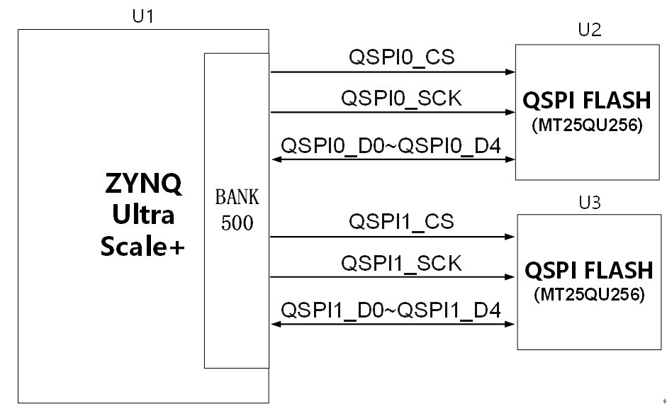
Figure 4.1 - QSPI Flash Connection Diagram
Configuration Chip Pin Assignment:
| Signal Name | Pin Name | Pin Number |
| MIO0_QSPI0_SCLK | PS_MIO0_500 | A24 |
| MIO1_QSPI0_IO1 | PS_MIO1_500 | C24 |
| MIO2_QSPI0_IO2 | PS_MIO2_500 | B24 |
| MIO3_QSPI0_IO3 | PS_MIO3_500 | E25 |
| MIO4_QSPI0_IO0 | PS_MIO4_500 | A25 |
| MIO5_QSPI0_SS_B | PS_MIO5_500 | D25 |
| MIO10_QSPI1_IO2 | PS_MIO10_500 | F26 |
| MIO11_QSPI1_IO3 | PS_MIO11_500 | B26 |
| MIO12_QSPI1_SCLK | PS_MIO12_500 | C27 |
| MIO7_QSPI1_SS_B | PS_MIO7_500 | B25 |
| MIO8_QSPI1_IO0 | PS_MIO8_500 | D26 |
| MIO9_QSPI1_IO1 | PS_MIO9_500 | C26 |
Table 4.2 - QSPI Flash Pin Assignment
eMMC FLASH
The BZ11 development board is equipped with one large-capacity 32GB eMMC FLASH chip, model MTFC32GBCAQTC-IT. It supports the HS-MMC interface of the JEDEC e-MMC V5.0 standard, with 1.8V or 3.3V signaling. The data width between the eMMC FLASH and the Zynq is 8 bits. Due to its large capacity and non-volatile nature, the eMMC FLASH can serve as a high-capacity storage device in the Zynq system, for example to store ARM applications, system files and other user data files. The specific model and related parameters of the eMMC FLASH are listed in Table 5.1.
| Ref. Designator | Chip Type | Capacity | Manufacturer |
| U8 | MTFC32GBCAQTC-IT | 32 GB | Micron |
Table 5.1 - eMMC Flash Model and Parameters
The eMMC FLASH is connected to the GPIO pins of PS BANK500 of the Zynq UltraScale+. In system design these PS GPIO pins must be configured as the eMMC interface. Figure 5.1 shows the eMMC FLASH in the schematic.
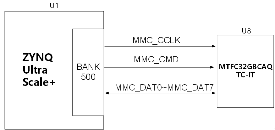
Figure 5.1 - eMMC Flash Connection Diagram
Configuration Chip Pin Assignment:
| Signal Name | Pin Name | Pin Number |
| MMC_CCLK | PS_MIO22_500 | F28 |
| MMC_CMD | PS_MIO21_500 | C28 |
| MMC_DAT0 | PS_MIO13_500 | D27 |
| MMC_DAT1 | PS_MIO14_500 | A27 |
| MMC_DAT2 | PS_MIO15_500 | E27 |
| MMC_DAT3 | PS_MIO16_500 | A28 |
| MMC_DAT4 | PS_MIO17_500 | C29 |
| MMC_DAT5 | PS_MIO18_500 | F27 |
| MMC_DAT6 | PS_MIO19_500 | B28 |
| MMC_DAT7 | PS_MIO20_500 | E29 |
| MMC_RSTN | PS_MIO23_500 | B29 |
Table 5.2 - eMMC Flash Pin Assignment
Clock Configuration
The BZ11 development board provides a reference clock and an RTC real-time clock for the PS. The clock circuit design is shown in Figure 6.1:
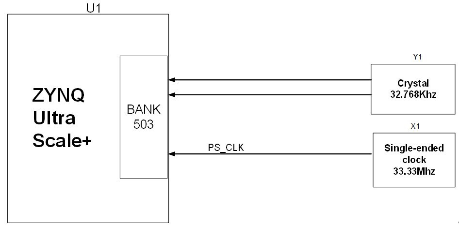
Figure 6.1 - Core Board Clock Sources
PS RTC Real-Time Clock
The passive crystal Y1 on the board provides a 32.768kHz real-time clock source for the PS, connected to the PS_PADI_503 and PS_PADO_503 pins of Zynq BANK503.
| Signal Name | Pin |
| PS_PADI_503 | M25 |
| PS_PADO_503 | L25 |
Table 6.1 - Clock Pin Assignment
PS Clock Source
The X1 oscillator on the board provides a 33.333MHz clock input for the PS. The clock input is connected to the PS_REF_CLK_503 pin of Zynq BANK503. Clock pin assignment:
| Signal Name | Pin |
| PS_REF_CLK | R24 |
Table 6.2 - Clock Pin Assignment
M.2 Interface
The BZ11 development board is equipped with one standard PCIe Gen2 x1 M.2 interface for connecting M.2 SSDs, at 5Gbps. The M.2 interface uses an M-key socket and supports PCIe only, not SATA; when selecting an SSD, users must choose a PCIe SSD.
The PCIe signals are connected directly to the PS BANK505 MGT transceivers of the ZU11EG. One pair of TX and RX signals is connected to one MGT lane as differential signals. The PCIe clock is provided by the Si5332 chip at 100MHz. The M.2 circuit design is shown in Figure 7.1:
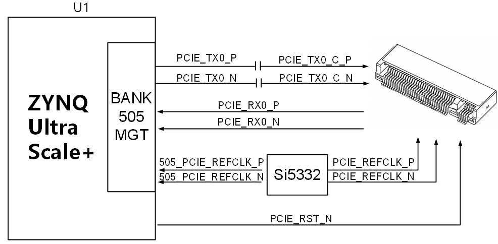
Figure 7.1 - M.2 Interface Design Diagram
The Zynq pin assignment of the M.2 interface is as follows:
| Signal Name | Pin Name | Pin Number | Remarks |
| PCIE_TX0_P | 505_TX0_P | U29 | PCIe Lane 0 Transmit Positive |
| PCIE_TX0_N | 505_TX0_N | U30 | PCIe Lane 0 Transmit Negative |
| PCIE_RX0_P | 505_RX0_P | U33 | PCIe Lane 0 Receive Positive |
| PCIE_RX0_N | 505_RX0_N | U34 | PCIe Lane 0 Receive Negative |
| PCIE_RST_N | PS_MIO37 | C33 | PCIe Reset Signal |
| PCIE_REFCLK_P | 505_CLK0_P | T27 | PCIe Reference Clock Positive |
| PCIE_REFCLK_N | 505_CLK0_N | T28 | PCIe Reference Clock Negative |
Table 7.1 - M.2 Interface Pin Assignment
DP Display Interface
The BZ11 development board provides one mini DisplayPort output interface for video image display. It supports the VESA DisplayPort V1.2a output standard, up to 4K x 2K@30Fps, and the Y-only, YCbCr444, YCbCr422, YCbCr420 and RGB video formats, with 6, 8, 10 or 12 bits per color.
The DisplayPort data lanes are driven directly by the PS MGT of ZU11EG BANK505; the LANE2 and LANE3 TX signals of the MGT are connected to the DP connector as differential signals. The DisplayPort auxiliary channel is connected to the MIO pins of the PS. The DP output interface design is shown in Figure 8.1:
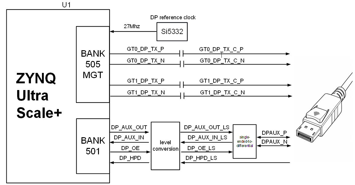
Figure 8.1 - DP Interface Design Diagram
The Zynq pin assignment of the DisplayPort interface is as follows:
| Signal Name | ZYNQ Pin Name | Pin Number | Remarks |
| GT0_DP_TX_N | 505_TX3_N | N30 | DP Data Low-Order Transmit Negative |
| GT0_DP_TX_P | 505_TX3_P | N29 | DP Data Low-Order Transmit Positive |
| GT1_DP_TX_N | 505_TX2_N | P32 | DP Data High-Order Transmit Negative |
| GT1_DP_TX_P | 505_TX2_P | P31 | DP Data High-Order Transmit Positive |
| 505_DP_CLKN | 505_CLK2_N | M32 | DP Reference Clock Negative |
| 505_DP_CLKP | 505_CLK2_P | M31 | DP Reference Clock Positive |
| DP_AUX_OUT_MIO27 | PS_MIO27 | A30 | DP Auxiliary Data Output |
| DP_AUX_IN_MIO30 | PS_MIO30 | A33 | DP Auxiliary Data Input |
| DP_OE_MIO29 | PS_MIO29 | A32 | DP Auxiliary Data Output Enable |
| DP_HPD_MIO28 | PS_MIO28 | A31 | DP Hot Plug Detect |
Table 8.1 - DisplayPort Pin Assignment
USB 3.0 Interface
The BZ11 development board has one USB 3.0 Type-C interface supporting HOST, SLAVE and OTG modes, with data transfer speeds of up to 5.0Gbps. USB 3.0 is connected through the PIPE3 interface, and USB 2.0 is connected to an external USB3320C chip through the ULPI interface, enabling high-speed USB 3.0 and USB 2.0 data communication. The USB 3.0 connection is shown in Figure 9.1:
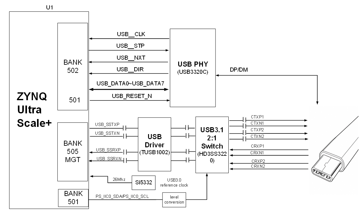
Figure 9.1 - USB 3.0 Interface Diagram
USB Interface Pin Assignment:
| Signal Name | Pin Name | Pin Number | Remarks |
| USB_SSTXN | 505_TX1_N | R30 | USB 3.0 Data Transmit Negative |
| USB_SSTXP | 505_TX1_P | R29 | USB 3.0 Data Transmit Positive |
| USB_SSRXN | 505_RX1_N | T32 | USB 3.0 Data Receive Negative |
| USB_SSRXP | 505_RX1_P | T31 | USB 3.0 Data Receive Positive |
| USB_DATA0 | PS_MIO56 | G34 | USB 2.0 Data Bit 0 |
| USB_DATA1 | PS_MIO57 | H29 | USB 2.0 Data Bit 1 |
| USB_DATA2 | PS_MIO54 | G31 | USB 2.0 Data Bit 2 |
| USB_DATA3 | PS_MIO59 | H32 | USB 2.0 Data Bit 3 |
| USB_DATA4 | PS_MIO60 | H33 | USB 2.0 Data Bit 4 |
| USB_DATA5 | PS_MIO61 | H34 | USB 2.0 Data Bit 5 |
| USB_DATA6 | PS_MIO62 | J29 | USB 2.0 Data Bit 6 |
| USB_DATA7 | PS_MIO63 | J30 | USB 2.0 Data Bit 7 |
| USB_STP | PS_MIO58 | H31 | USB 2.0 Stop Signal |
| USB_DIR | PS_MIO53 | G30 | USB 2.0 Data Direction Signal |
| USB_CLK | PS_MIO52 | G29 | USB 2.0 Clock Signal |
| USB_NXT | PS_MIO55 | G33 | USB 2.0 Next Data Signal |
| USB_RESET_N | PS_MIO26 | A29 | USB 2.0 Reset Signal |
| PS_IIC0_SCL | PS_MIO34 | B34 | I2C Clock Signal |
| PS_IIC0_SDA | PS_MIO35 | C31 | I2C Data Signal |
Table 9.1 - USB Interface Pin Assignment
Gigabit Ethernet Interface
The BZ11 development board has one Gigabit Ethernet interface connected to the PS. The Ethernet chip is MICROCHIP's industrial-grade Ethernet PHY chip (KSZ9031RNX), providing network communication for users. The PS-side Ethernet PHY is connected to the GPIO interface of PS BANK502 of the Zynq. The KSZ9031RNX supports 10/100/1000 Mbps network rates and communicates with the MAC layer of the Zynq system through the RGMII interface. It supports MDI/MDX auto-adaptation, speed auto-adaptation and Master/SLAVE auto-adaptation, and supports the MDIO bus for PHY register management.
On power-up, the KSZ9031RNX detects the level states of certain IOs to determine its operating mode. Table 10.1 describes the default settings of the PHY chip after power-up.
| Configuration Pin | Description | Configuration Value |
| RXD3_ADR0 RXC_ADR1 RXCTL_ADR2 | PHY Address in MDIO/MDC Mode | PHY Address = 001 |
| RXD1_TXDLY | TX Clock 2ns Delay | Delay |
| RXD0_RXDLY | RX Clock 2ns Delay | Delay |
Table 10.1 - PHY Chip Default Configuration Values
At Gigabit Ethernet, data between the Zynq and the KSZ9031RNX PHY is transferred over the RGMII bus with a 125MHz clock, and data is sampled on both the rising and falling edges of the clock.
At 100 Mbps Ethernet, data between the Zynq and the KSZ9031RNX PHY is transferred over the RGMII bus with a 25MHz clock, and data is sampled on both the rising and falling edges of the clock. Figure 10.1 shows the connection of the Zynq Ethernet PHY1 chip:
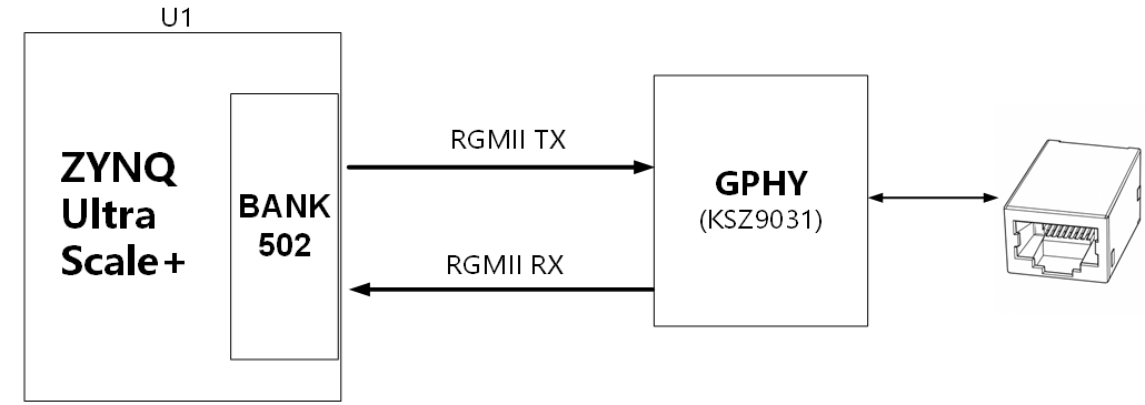
Figure 10.1 - ZYNQ and GPHY Connection Diagram
PS Gigabit Ethernet pin assignment is as follows:
| Signal Name | Pin Name | Pin Number | Remarks |
| PHY1_TXCK | PHY1_TXCK | J31 | Ethernet 1 RGMII Transmit Clock |
| PHY1_TXD0 | PHY1_TXD0 | J32 | Ethernet 1 Transmit Data Bit 0 |
| PHY1_TXD1 | PHY1_TXD1 | J34 | Ethernet 1 Transmit Data Bit 1 |
| PHY1_TXD2 | PHY1_TXD2 | K28 | Ethernet 1 Transmit Data Bit 2 |
| PHY1_TXD3 | PHY1_TXD3 | K29 | Ethernet 1 Transmit Data Bit 3 |
| PHY1_TXCTL | PHY1_TXCTL | K30 | Ethernet 1 Transmit Enable Signal |
| PHY1_RXCK | PHY1_RXCK | K31 | Ethernet 1 RGMII Receive Clock |
| PHY1_RXD0 | PHY1_RXD0 | K32 | Ethernet 1 Receive Data Bit 0 |
| PHY1_RXD1 | PHY1_RXD1 | K33 | Ethernet 1 Receive Data Bit 1 |
| PHY1_RXD2 | PHY1_RXD2 | K34 | Ethernet 1 Receive Data Bit 2 |
| PHY1_RXD3 | PHY1_RXD3 | L29 | Ethernet 1 Receive Data Bit 3 |
| PHY1_RXCTL | PHY1_RXCTL | L30 | Ethernet 1 Receive Data Valid Signal |
| PHY1_MDC | PHY1_MDC | L33 | Ethernet 1 MDIO Management Clock |
| PHY1_MDIO | PHY1_MDIO | L34 | Ethernet 1 MDIO Management Data |
Table 10.2 - PS Gigabit Ethernet Pin Assignment
UART Serial Interface
The BZ11 development board provides one UART interface connected to the PS, extended externally through a 3-pin 2.54mm pitch socket. It can be connected to the USB port of a PC with a TTL-to-USB cable for serial data communication. The UART circuit design is shown below:
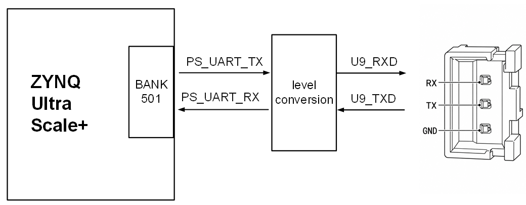
Figure 11.1 - USB-to-Serial Diagram
Zynq pin assignment of the serial port:
| Signal Name | Pin Name | Pin Number | Remarks |
| PS_UART_RX | PS_MIO42 | D34 | PS UART Data Input |
| PS_UART_TX | PS_MIO43 | E30 | PS UART Data Output |
Table 11.1 - USB-to-Serial Pin Assignment
Micro SD Card Socket
The BZ11 development board includes one Micro SD card socket, providing user access to Micro SD card storage for the ZU11EG BOOT program, the Linux operating system kernel, the file system and other user data files.
The SDIO signals are connected to the PS BANK501 IO signals of the ZU11EG. Because the VCCIO of BANK501 is set to 1.8V while Micro SD cards use 3.3V data levels, a TXS02612 level shifter is used here. The schematic of the ZU11EG PS and the Micro SD card connector is shown in Figure 12.1.
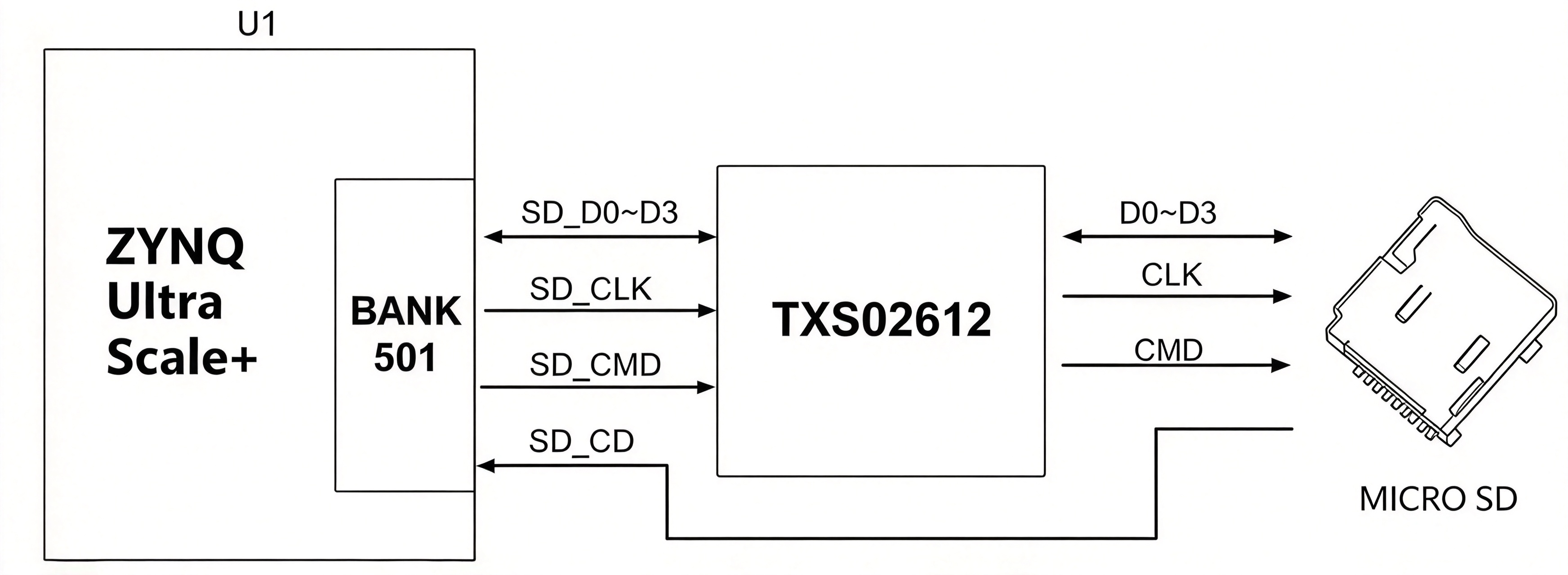
Figure 12.1 - SD Card Connection Diagram
Micro SD Card Socket Pin Assignment
| Signal Name | Pin Name | Pin Number | Remarks |
| SD_CLK | SD_CLK | F34 | SD Clock Signal |
| SD_CD | SD_CD | E33 | SD Detect Signal |
| SD_D0 | SD_D0 | E34 | SD Data Data0 |
| SD_D1 | SD_D1 | F30 | SD Data Data1 |
| SD_D2 | SD_D2 | F31 | SD Data Data2 |
| SD_D3 | SD_D3 | F32 | SD Data Data3 |
| SD_CMD | SD_CMD | F33 | SD Card Command Signal |
Table 12.1 - SD Card Socket Pin Assignment
QSFP+ Fiber Optic Interface
The BZ11 development board has a small-form-factor pluggable QSFP+ fiber optic interface. The optical transceiver integrates 4 transmit channels and 4 receive channels, and this 4-channel pluggable interface reaches a transmission rate of 40Gbps, meeting the demand for higher-density, high-speed pluggable optical communication solutions.
The QSFP+ optical transceiver signals are connected directly to the GTH transceivers of FPGA BANK228. The four TX and RX channels of the optical interface are connected directly to the GTH transceivers; since a single GTH lane supports up to 10Gbps bandwidth, the four GTH lanes can reach 40Gbps. The reference clock of the BANK228 GTH transceivers is provided by a 156.25MHz differential oscillator. The QSFP+ optical design of the development board is shown in Figure 13.1, where the optical module control signals are connected to FPGA BANK64.
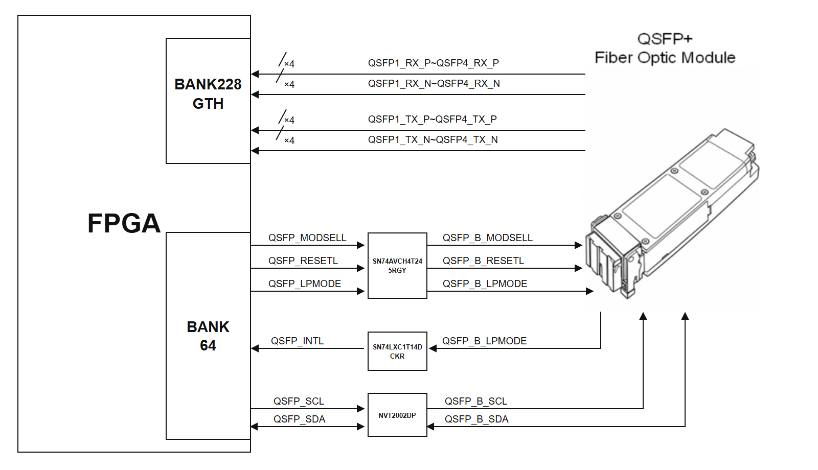
Figure 13.1 - QSFP+ Fiber Optic Design Diagram
FPGA pin assignment of the QSFP+ fiber optic interface is as follows:
| Net Name | Pin Name | FPGA Pin | Remarks |
| QSFP1_TX1_P | 228_TX0_P | M4 | QSFP+ Channel 1 Data Transmit Positive |
| QSFP1_TX1_N | 228_TX0_N | M3 | QSFP+ Channel 1 Data Transmit Negative |
| QSFP1_TX2_P | 228_TX1_P | L6 | QSFP+ Channel 2 Data Transmit Positive |
| QSFP1_TX2_N | 228_TX1_N | L5 | QSFP+ Channel 2 Data Transmit Negative |
| QSFP1_TX3_P | 228_TX2_P | K4 | QSFP+ Channel 3 Data Transmit Positive |
| QSFP1_TX3_N | 228_TX2_N | K3 | QSFP+ Channel 3 Data Transmit Negative |
| QSFP1_TX4_P | 228_TX3_P | H4 | QSFP+ Channel 4 Data Transmit Positive |
| QSFP1_TX4_N | 228_TX3_N | H3 | QSFP+ Channel 4 Data Transmit Negative |
| QSFP1_RX1_P | 228_RX0_P | N2 | QSFP+ Channel 1 Data Receive Positive |
| QSFP1_RX1_N | 228_RX0_N | N1 | QSFP+ Channel 1 Data Receive Negative |
| QSFP1_RX2_P | 228_RX1_P | L2 | QSFP+ Channel 2 Data Receive Positive |
| QSFP1_RX2_N | 228_RX1_N | L1 | QSFP+ Channel 2 Data Receive Negative |
| QSFP1_RX3_P | 228_RX2_P | J2 | QSFP+ Channel 3 Data Receive Positive |
| QSFP1_RX3_N | 228_RX2_N | J1 | QSFP+ Channel 3 Data Receive Negative |
| QSFP1_RX4_P | 228_RX3_P | G2 | QSFP+ Channel 4 Data Receive Positive |
| QSFP1_RX4_N | 228_RX3_N | G1 | QSFP+ Channel 4 Data Receive Negative |
| QSFP_MODSELL | B64_IO_L5N | AP15 | Mode Select, low level enables I2C |
| QSFP_RESETL | B64_IO_L5P | AP16 | Reset Signal, active low |
| QSFP_INTL | B64_IO_L6N | AN16 | Interrupt Signal, active low |
| QSFP_LPMODE | B64_IO_L6P | AN17 | Low Power Mode Select |
| QSFP_SCL | B64_IO_T1U | AL17 | I2C Clock Signal |
| QSFP_SDA | B64_IO_T2U | AH16 | I2C Data Signal |
Table 13.1 - QSFP+ Fiber Optic Interface Pin Assignment
FMC Connectors
The BZ11 development board has four standard FMC HPC expansion connectors, which can be connected to FMC modules from Xilinx or ALINX (HDMI input/output module, dual-camera module, high-speed AD module, etc.). Because the FPGA does not have enough pins, not all FMC connectors are connected to the FPGA, so not all FMC modules can be used; which module can be used must be evaluated with reference to the schematic design. The hardware connection between the four FMC connectors and the FPGA is shown in Figure 14.1.
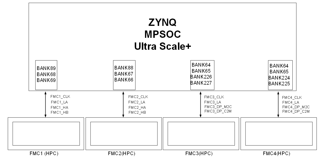
Figure 14.1 - FMC Connector Connection Diagram
The pin assignment of the FMC1 connector is as follows:
| FMC Pin Number | Net Name | ZYNQ Pin Number |
| G3 | FMC1_CLK0_C2M_N | F10 |
| G2 | FMC1_CLK0_C2M_P | G10 |
| H5 | FMC1_CLK0_M2C_N | E14 |
| H4 | FMC1_CLK0_M2C_P | E15 |
| K4 | FMC1_CLK1_M2C_P | H14 |
| F5 | FMC1_HA00_N | E5 |
| F4 | FMC1_HA00_P | F6 |
| K8 | FMC1_HA02_N | B1 |
| K7 | FMC1_HA02_P | C1 |
| J7 | FMC1_HA03_N | C2 |
| J6 | FMC1_HA03_P | D2 |
| F8 | FMC1_HA04_N | F4 |
| F7 | FMC1_HA04_P | F5 |
| E7 | FMC1_HA05_N | D4 |
| E6 | FMC1_HA05_P | E4 |
| K11 | FMC1_HA06_N | A2 |
| K10 | FMC1_HA06_P | A3 |
| J10 | FMC1_HA07_N | B3 |
| J9 | FMC1_HA07_P | C3 |
| F11 | FMC1_HA08_N | B4 |
| F10 | FMC1_HA08_P | C4 |
| J13 | FMC1_HA11_N | E2 |
| J12 | FMC1_HA11_P | E3 |
| F14 | FMC1_HA12_N | A5 |
| F13 | FMC1_HA12_P | B5 |
| E13 | FMC1_HA13_N | D5 |
| E12 | FMC1_HA13_P | D6 |
| J16 | FMC1_HA14_N | D1 |
| J15 | FMC1_HA14_P | E1 |
| F17 | FMC1_HA15_N | J19 |
| F16 | FMC1_HA15_P | J20 |
| E16 | FMC1_HA16_N | L16 |
| E15 | FMC1_HA16_P | L17 |
| K17 | FMC1_HA17_N | G13 |
| K16 | FMC1_HA17_P | A9 |
| K13 | FMC1_HA10_P | D7 |
| E10 | FMC1_HA09_N | A11 |
| E9 | FMC1_HA09_P | B11 |
| J21 | FMC1_HA22_P | E13 |
| K26 | FMC1_HB00_CC_N | L13 |
| K25 | FMC1_HB00_CC_P | M13 |
| J25 | FMC1_HB01_N | J11 |
| J24 | FMC1_HB01_P | K12 |
| F23 | FMC1_HB02_N | J14 |
| F22 | FMC1_HB02_P | K14 |
| E22 | FMC1_HB03_N | J10 |
| E21 | FMC1_HB03_P | K10 |
| F26 | FMC1_HB04_N | L11 |
| F25 | FMC1_HB04_P | L12 |
| E25 | FMC1_HB05_N | B15 |
| E24 | FMC1_HB05_P | B16 |
| K29 | FMC1_HB06_CC_N | A12 |
| K28 | FMC1_HB06_CC_P | A13 |
| J28 | FMC1_HB07_N | B13 |
| J27 | FMC1_HB07_P | B14 |
| F29 | FMC1_HB08_N | A14 |
| F28 | FMC1_HB08_P | A15 |
| E28 | FMC1_HB09_N | A16 |
| E27 | FMC1_HB09_P | A17 |
| G7 | FMC1_LA00_CC_N | F15 |
| G6 | FMC1_LA00_CC_P | G15 |
| D9 | FMC1_LA01_CC_N | F16 |
| D8 | FMC1_LA01_CC_P | F17 |
| H8 | FMC1_LA02_N | G19 |
| H7 | FMC1_LA02_P | H19 |
| G10 | FMC1_LA03_N | G16 |
| G9 | FMC1_LA03_P | H16 |
| H11 | FMC1_LA04_N | F18 |
| H10 | FMC1_LA04_P | G18 |
| D12 | FMC1_LA05_N | H17 |
| D11 | FMC1_LA05_P | H18 |
| C11 | FMC1_LA06_N | K15 |
| C10 | FMC1_LA06_P | L15 |
| H14 | FMC1_LA07_N | K18 |
| H13 | FMC1_LA07_P | K19 |
| G13 | FMC1_LA08_N | J17 |
| G12 | FMC1_LA08_P | K17 |
| D15 | FMC1_LA09_N | J15 |
| D14 | FMC1_LA09_P | J16 |
| C15 | FMC1_LA10_N | C12 |
| C14 | FMC1_LA10_P | C13 |
| H17 | FMC1_LA11_N | E17 |
| H16 | FMC1_LA11_P | E18 |
| G16 | FMC1_LA12_N | K20 |
| G15 | FMC1_LA12_P | L20 |
| D18 | FMC1_LA13_N | C17 |
| D17 | FMC1_LA13_P | D17 |
| C19 | FMC1_LA14_N | C16 |
| C18 | FMC1_LA14_P | D16 |
| H20 | FMC1_LA15_N | F13 |
| H19 | FMC1_LA15_P | G14 |
| G19 | FMC1_LA16_N | D14 |
| G18 | FMC1_LA16_P | D15 |
| D21 | FMC1_LA17_CC_N | E10 |
| D20 | FMC1_LA17_CC_P | F11 |
| C23 | FMC1_LA18_CC_N | G11 |
| C22 | FMC1_LA18_CC_P | H11 |
| H23 | FMC1_LA19_N | C11 |
| H22 | FMC1_LA19_P | D12 |
| G22 | FMC1_LA20_N | D10 |
| G21 | FMC1_LA20_P | D11 |
| H26 | FMC1_LA21_N | A6 |
| H25 | FMC1_LA21_P | B6 |
| G25 | FMC1_LA22_N | B8 |
| G24 | FMC1_LA22_P | B9 |
| D24 | FMC1_LA23_N | A10 |
| D23 | FMC1_LA23_P | B10 |
| H29 | FMC1_LA24_N | E12 |
| H28 | FMC1_LA24_P | F12 |
| G28 | FMC1_LA25_N | K13 |
| G27 | FMC1_LA25_P | L14 |
| D27 | FMC1_LA26_N | C6 |
| D26 | FMC1_LA26_P | C7 |
| C27 | FMC1_LA27_N | A7 |
| C26 | FMC1_LA27_P | A8 |
| H32 | FMC1_LA28_N | H12 |
| H31 | FMC1_LA28_P | H13 |
| G31 | FMC1_LA29_N | E7 |
| G30 | FMC1_LA29_P | F7 |
| H35 | FMC1_LA30_N | C8 |
| H34 | FMC1_LA30_P | C9 |
| G34 | FMC1_LA31_N | E8 |
| G33 | FMC1_LA31_P | F8 |
| H38 | FMC1_LA32_N | D9 |
| H37 | FMC1_LA32_P | E9 |
| G37 | FMC1_LA33_N | G9 |
| G36 | FMC1_LA33_P | H9 |
Table 14.1 - FMC1 Connector Pin Assignment
The pin assignment of the FMC2 connector is as follows:
| FMC Pin Number | Net Name | ZYNQ Pin Number |
| G3 | FMC2_CLK0_C2M_N | AK9 |
| G2 | FMC2_CLK0_C2M_P | AJ9 |
| H5 | FMC2_CLK0_M2C_N | F21 |
| H4 | FMC2_CLK0_M2C_P | G21 |
| K4 | FMC2_CLK1_M2C_P | E20 |
| F5 | FMC2_HA00_N | G6 |
| F4 | FMC2_HA00_P | H6 |
| K8 | FMC2_HA02_N | G8 |
| K7 | FMC2_HA02_P | H8 |
| J7 | FMC2_HA03_N | J9 |
| J6 | FMC2_HA03_P | K9 |
| F8 | FMC2_HA04_N | K8 |
| F7 | FMC2_HA04_P | L8 |
| E7 | FMC2_HA05_N | J6 |
| E6 | FMC2_HA05_P | J7 |
| K11 | FMC2_HA06_N | N12 |
| K10 | FMC2_HA06_P | P12 |
| J10 | FMC2_HA07_N | L10 |
| J9 | FMC2_HA07_P | M10 |
| F11 | FMC2_HA08_N | M8 |
| F10 | FMC2_HA08_P | M9 |
| E10 | FMC2_HA09_N | AP8 |
| E9 | FMC2_HA09_P | AM13 |
| J13 | FMC2_HA11_N | G7 |
| J12 | FMC2_HA11_P | H7 |
| F14 | FMC2_HA12_N | M11 |
| F13 | FMC2_HA12_P | N11 |
| E13 | FMC2_HA13_N | N8 |
| E12 | FMC2_HA13_P | N9 |
| J16 | FMC2_HA14_N | M12 |
| J15 | FMC2_HA14_P | N13 |
| F17 | FMC2_HA15_N | AC13 |
| F16 | FMC2_HA15_P | AB13 |
| E16 | FMC2_HA16_N | B21 |
| E15 | FMC2_HA16_P | B20 |
| K17 | FMC2_HA17_N | AH8 |
| K16 | FMC2_HA17_P | AC14 |
| K13 | FMC2_HA10_P | F25 |
| J21 | FMC2_HA22_P | B23 |
| K26 | FMC2_HB00_CC_N | L22 |
| K25 | FMC2_HB00_CC_P | L21 |
| J25 | FMC2_HB01_N | K24 |
| J24 | FMC2_HB01_P | L23 |
| F23 | FMC2_HB02_N | K23 |
| F22 | FMC2_HB02_P | K22 |
| E22 | FMC2_HB03_N | J22 |
| E21 | FMC2_HB03_P | J21 |
| F26 | FMC2_HB04_N | H26 |
| F25 | FMC2_HB04_P | J25 |
| E25 | FMC2_HB05_N | AF12 |
| E24 | FMC2_HB05_P | AE12 |
| K29 | FMC2_HB06_CC_N | AD12 |
| K28 | FMC2_HB06_CC_P | AC12 |
| J28 | FMC2_HB07_N | AF13 |
| J27 | FMC2_HB07_P | AE13 |
| F29 | FMC2_HB08_N | AE14 |
| F28 | FMC2_HB08_P | AD14 |
| E28 | FMC2_HB09_N | AF10 |
| E27 | FMC2_HB09_P | AF11 |
| G7 | FMC2_LA00_CC_N | G24 |
| G6 | FMC2_LA00_CC_P | G23 |
| D9 | FMC2_LA01_CC_N | E23 |
| D8 | FMC2_LA01_CC_P | F23 |
| H8 | FMC2_LA02_N | D24 |
| H7 | FMC2_LA02_P | E24 |
| G10 | FMC2_LA03_N | G26 |
| G9 | FMC2_LA03_P | G25 |
| H11 | FMC2_LA04_N | C22 |
| H10 | FMC2_LA04_P | C21 |
| D12 | FMC2_LA05_N | C23 |
| D11 | FMC2_LA05_P | D22 |
| C11 | FMC2_LA06_N | A23 |
| C10 | FMC2_LA06_P | A22 |
| H14 | FMC2_LA07_N | B19 |
| H13 | FMC2_LA07_P | B18 |
| G13 | FMC2_LA08_N | A21 |
| G12 | FMC2_LA08_P | A20 |
| D15 | FMC2_LA09_N | C19 |
| D14 | FMC2_LA09_P | C18 |
| C15 | FMC2_LA10_N | H24 |
| C14 | FMC2_LA10_P | J24 |
| H17 | FMC2_LA11_N | D21 |
| H16 | FMC2_LA11_P | D20 |
| G16 | FMC2_LA12_N | A19 |
| G15 | FMC2_LA12_P | A18 |
| D18 | FMC2_LA13_N | H22 |
| D17 | FMC2_LA13_P | H21 |
| C19 | FMC2_LA14_N | D19 |
| C18 | FMC2_LA14_P | E19 |
| H20 | FMC2_LA15_N | F20 |
| H19 | FMC2_LA15_P | G20 |
| G19 | FMC2_LA16_N | E22 |
| G18 | FMC2_LA16_P | F22 |
| D21 | FMC2_LA17_CC_N | AJ11 |
| D20 | FMC2_LA17_CC_P | AH11 |
| C23 | FMC2_LA18_CC_N | AJ12 |
| C22 | FMC2_LA18_CC_P | AH12 |
| H23 | FMC2_LA19_N | AG8 |
| H22 | FMC2_LA19_P | AF8 |
| G22 | FMC2_LA20_N | AG10 |
| G21 | FMC2_LA20_P | AG11 |
| H26 | FMC2_LA21_N | AL8 |
| H25 | FMC2_LA21_P | AK8 |
| G25 | FMC2_LA22_N | AK10 |
| G24 | FMC2_LA22_P | AJ10 |
| D24 | FMC2_LA23_N | AL12 |
| D23 | FMC2_LA23_P | AK12 |
| H29 | FMC2_LA24_N | AH9 |
| H28 | FMC2_LA24_P | AG9 |
| G28 | FMC2_LA25_N | AM8 |
| G27 | FMC2_LA25_P | AM9 |
| D27 | FMC2_LA26_N | AL13 |
| D26 | FMC2_LA26_P | AK13 |
| C27 | FMC2_LA27_N | AL10 |
| C26 | FMC2_LA27_P | AL11 |
| H32 | FMC2_LA28_N | AH13 |
| H31 | FMC2_LA28_P | AG13 |
| G31 | FMC2_LA29_N | AP12 |
| G30 | FMC2_LA29_P | AN12 |
| H35 | FMC2_LA30_N | AN8 |
| H34 | FMC2_LA30_P | AN9 |
| G34 | FMC2_LA31_N | AM10 |
| G33 | FMC2_LA31_P | AM11 |
| H38 | FMC2_LA32_N | AP11 |
| H37 | FMC2_LA32_P | AN11 |
| G37 | FMC2_LA33_N | AP9 |
| G36 | FMC2_LA33_P | AP10 |
Table 14.2 - FMC2 Connector Pin Assignment
The pin assignment of the FMC3 connector is as follows:
| FMC Pin Number | Net Name | ZYNQ Pin Number |
| G3 | FMC3_CLK0_C2M_N | AJ22 |
| G2 | FMC3_CLK0_C2M_P | AJ21 |
| H5 | FMC3_CLK0_M2C_N | AJ15 |
| H4 | FMC3_CLK0_M2C_P | AJ16 |
| C3 | FMC3_DP0_C2M_N | U5 |
| C2 | FMC3_DP0_C2M_P | U6 |
| C7 | FMC3_DP0_M2C_N | V3 |
| C6 | FMC3_DP0_M2C_P | V4 |
| A23 | FMC3_DP1_C2M_N | T3 |
| A22 | FMC3_DP1_C2M_P | T4 |
| A3 | FMC3_DP1_M2C_N | U1 |
| A2 | FMC3_DP1_M2C_P | U2 |
| A27 | FMC3_DP2_C2M_N | R5 |
| A26 | FMC3_DP2_C2M_P | R6 |
| A7 | FMC3_DP2_M2C_N | R1 |
| A6 | FMC3_DP2_M2C_P | R2 |
| A31 | FMC3_DP3_C2M_N | N5 |
| A30 | FMC3_DP3_C2M_P | N6 |
| A11 | FMC3_DP3_M2C_N | P3 |
| A10 | FMC3_DP3_M2C_P | P4 |
| A35 | FMC3_DP4_C2M_N | AC5 |
| A34 | FMC3_DP4_C2M_P | AC6 |
| A15 | FMC3_DP4_M2C_N | AC1 |
| A14 | FMC3_DP4_M2C_P | AC2 |
| A39 | FMC3_DP5_C2M_N | AA5 |
| A38 | FMC3_DP5_C2M_P | AA6 |
| A19 | FMC3_DP5_M2C_N | AB3 |
| A18 | FMC3_DP5_M2C_P | AB4 |
| B37 | FMC3_DP6_C2M_N | Y3 |
| B36 | FMC3_DP6_C2M_P | Y4 |
| B17 | FMC3_DP6_M2C_N | AA1 |
| B16 | FMC3_DP6_M2C_P | AA2 |
| B33 | FMC3_DP7_C2M_N | W5 |
| B32 | FMC3_DP7_C2M_P | W6 |
| B13 | FMC3_DP7_M2C_N | W1 |
| B12 | FMC3_DP7_M2C_P | W2 |
| G7 | FMC3_LA00_CC_N | AG18 |
| G6 | FMC3_LA00_CC_P | AF18 |
| D9 | FMC3_LA01_CC_N | AH17 |
| D8 | FMC3_LA01_CC_P | AH18 |
| H8 | FMC3_LA02_N | AJ14 |
| H7 | FMC3_LA02_P | AH14 |
| G10 | FMC3_LA03_N | AG14 |
| G9 | FMC3_LA03_P | AG15 |
| H11 | FMC3_LA04_N | AF15 |
| H10 | FMC3_LA04_P | AF16 |
| D12 | FMC3_LA05_N | AF17 |
| D11 | FMC3_LA05_P | AE17 |
| C11 | FMC3_LA06_N | AA15 |
| C10 | FMC3_LA06_P | AA16 |
| H14 | FMC3_LA07_N | AB15 |
| H13 | FMC3_LA07_P | AB16 |
| G13 | FMC3_LA08_N | AB14 |
| G12 | FMC3_LA08_P | AA14 |
| D15 | FMC3_LA09_N | AC16 |
| D14 | FMC3_LA09_P | AC17 |
| C15 | FMC3_LA10_N | AD16 |
| C14 | FMC3_LA10_P | AD17 |
| H17 | FMC3_LA11_N | AL18 |
| H16 | FMC3_LA11_P | AK18 |
| G16 | FMC3_LA12_N | AE15 |
| G15 | FMC3_LA12_P | AD15 |
| D18 | FMC3_LA13_N | AK14 |
| D17 | FMC3_LA13_P | AK15 |
| C19 | FMC3_LA14_N | AM15 |
| C18 | FMC3_LA14_P | AM16 |
| H20 | FMC3_LA15_N | AL15 |
| H19 | FMC3_LA15_P | AL16 |
| G19 | FMC3_LA16_N | AK17 |
| G18 | FMC3_LA16_P | AJ17 |
| D21 | FMC3_LA17_CC_N | AH21 |
| D20 | FMC3_LA17_CC_P | AG21 |
| C23 | FMC3_LA18_CC_N | AH23 |
| C22 | FMC3_LA18_CC_P | AH22 |
| H23 | FMC3_LA19_N | AN19 |
| H22 | FMC3_LA19_P | AM19 |
| G22 | FMC3_LA20_N | AF22 |
| G21 | FMC3_LA20_P | AF21 |
| H26 | FMC3_LA21_N | AB18 |
| H25 | FMC3_LA21_P | AA18 |
| G25 | FMC3_LA22_N | AC19 |
| G24 | FMC3_LA22_P | AB19 |
| D24 | FMC3_LA23_N | AD19 |
| D23 | FMC3_LA23_P | AC18 |
| H29 | FMC3_LA24_N | AG20 |
| H28 | FMC3_LA24_P | AG19 |
| G28 | FMC3_LA25_N | AA20 |
| G27 | FMC3_LA25_P | AA19 |
| D27 | FMC3_LA26_N | AE19 |
| D26 | FMC3_LA26_P | AE18 |
| C27 | FMC3_LA27_N | AE20 |
| C26 | FMC3_LA27_P | AD20 |
| H32 | FMC3_LA28_N | AG23 |
| H31 | FMC3_LA28_P | AF23 |
| G31 | FMC3_LA29_N | AL21 |
| G30 | FMC3_LA29_P | AL20 |
| H35 | FMC3_LA30_N | AK19 |
| H34 | FMC3_LA30_P | AJ19 |
| G34 | FMC3_LA31_N | AK20 |
| G33 | FMC3_LA31_P | AJ20 |
| H38 | FMC3_LA32_N | AK23 |
| H37 | FMC3_LA32_P | AK22 |
| G37 | FMC3_LA33_N | AL23 |
| G36 | FMC3_LA33_P | AL22 |
| D5 | FMC3_GBTCLK0_M2C_N | W9 |
| D4 | FMC3_GBTCLK0_M2C_P | W10 |
| B21 | FMC3_GBTCLK1_M2C_N | Y7 |
| B20 | FMC3_GBTCLK1_M2C_P | Y8 |
Table 14.3 - FMC3 Connector Pin Assignment
The pin assignment of the FMC4 connector is as follows:
| FMC Pin Number | Net Name | ZYNQ Pin Number |
| D5 | FMC4_GBTCLK0_M2C_N | AC9 |
| D4 | FMC4_GBTCLK0_M2C_P | AC10 |
| B21 | FMC4_GBTCLK1_M2C_N | AD7 |
| B20 | FMC4_GBTCLK1_M2C_P | AD8 |
| C3 | FMC4_DP0_C2M_N | AD3 |
| C2 | FMC4_DP0_C2M_P | AD4 |
| C7 | FMC4_DP0_M2C_N | AE1 |
| C6 | FMC4_DP0_M2C_P | AE2 |
| A23 | FMC4_DP1_C2M_N | AE5 |
| A22 | FMC4_DP1_C2M_P | AE6 |
| A3 | FMC4_DP1_M2C_N | AF3 |
| A2 | FMC4_DP1_M2C_P | AF4 |
| A27 | FMC4_DP2_C2M_N | AG5 |
| A26 | FMC4_DP2_C2M_P | AG6 |
| A7 | FMC4_DP2_M2C_N | AG1 |
| A6 | FMC4_DP2_M2C_P | AG2 |
| A31 | FMC4_DP3_C2M_N | AH3 |
| A30 | FMC4_DP3_C2M_P | AH4 |
| A11 | FMC4_DP3_M2C_N | AJ1 |
| A10 | FMC4_DP3_M2C_P | AJ2 |
| A35 | FMC4_DP4_C2M_N | AN5 |
| A34 | FMC4_DP4_C2M_P | AN6 |
| A15 | FMC4_DP4_M2C_N | AP3 |
| A14 | FMC4_DP4_M2C_P | AP4 |
| A39 | FMC4_DP5_C2M_N | AM3 |
| A38 | FMC4_DP5_C2M_P | AM4 |
| A19 | FMC4_DP5_M2C_N | AN1 |
| A18 | FMC4_DP5_M2C_P | AN2 |
| B37 | FMC4_DP6_C2M_N | AL5 |
| B36 | FMC4_DP6_C2M_P | AL6 |
| B17 | FMC4_DP6_M2C_N | AL1 |
| B16 | FMC4_DP6_M2C_P | AL2 |
| B33 | FMC4_DP7_C2M_N | AJ5 |
| B32 | FMC4_DP7_C2M_P | AJ6 |
| B13 | FMC4_DP7_M2C_N | AK3 |
| B12 | FMC4_DP7_M2C_P | AK4 |
| H8 | FMC4_LA02_N | AN18 |
| H7 | FMC4_LA02_P | AM18 |
| G10 | FMC4_LA03_N | AP17 |
| G9 | FMC4_LA03_P | AP18 |
| G13 | FMC4_LA08_N | AN14 |
| G12 | FMC4_LA08_P | AM14 |
| G16 | FMC4_LA12_N | AP13 |
| G15 | FMC4_LA12_P | AN13 |
| H20 | FMC4_LA15_N | AP20 |
| H19 | FMC4_LA15_P | AP19 |
| H23 | FMC4_LA19_N | AN21 |
| H22 | FMC4_LA19_P | AM21 |
| H26 | FMC4_LA21_N | AP23 |
| H25 | FMC4_LA21_P | AN22 |
| G25 | FMC4_LA22_N | AP22 |
| G24 | FMC4_LA22_P | AP21 |
| G28 | FMC4_LA25_N | AN23 |
| G27 | FMC4_LA25_P | AM23 |
| G31 | FMC4_LA29_N | AE24 |
| G30 | FMC4_LA29_P | AE23 |
Table 14.4 - FMC4 Connector Pin Assignment
JTAG Debug Port
A JTAG interface is reserved on the BZ11 development board for downloading Zynq UltraScale+ programs or programming the FLASH. To avoid damage to the Zynq UltraScale+ chip caused by hot plugging, protection diodes are added on the JTAG signals to keep the signal voltage within the range accepted by the FPGA.
EEPROM
The BZ11 development board has an onboard EEPROM, model 24LC04, with a capacity of 4Kbit (22568 bits), connected to the PS through the I2C bus for communication. The EEPROM and the temperature sensor are mounted on the I2C bus of Zynq UltraScale+ BANK501 MIO. Figure 16.1 shows the schematic of the EEPROM and the temperature sensor:
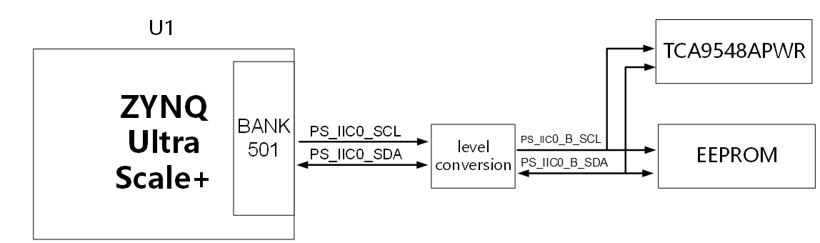
Figure 16.1 - EEPROM and Sensor Schematic
EEPROM communication pin assignment is as follows:
| Signal Name | Pin Name | Pin Number | Remarks |
| PS_IIC0_SCL | PS_MIO34 | B34 | I2C Clock Signal |
| PS_IIC0_SDA | PS_MIO35 | C31 | I2C Data Signal |
Table 16.1 - EEPROM Communication Pin Assignment
LEDs
The BZ11 development board has 4 LEDs and 2 dual-layer LEDs, including one power indicator, one DONE indicator, and PS control indicators connected to the dual-layer LEDs, plus two user indicators. Users can switch them on and off through programs. The hardware connection of the user LEDs is shown in Figure 17.1:
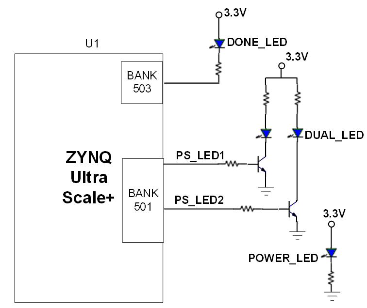
Figure 17.1 - User LED Hardware Connection Diagram
User LED Pin Assignment
| Signal Name | Pin Name | Pin Number | Remarks |
| PS_LED1 | PS_MIO44 | E32 | User PS LED 1 |
| PS_LED2 | PS_MIO38 | C34 | User PS LED 2 |
Table 17.1 - User LED Pin Assignment
Button
The BZ11 development board has one RESET button whose reset signal is connected to the MIO of the PS; users can use this button to reset the Zynq system. The reset button is active low. The button connection is shown in Figure 18.1:
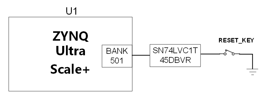
Figure 18.1 - Reset Button Connection Diagram
Zynq Pin Assignment of the Button
| Signal Name | Pin Name | Pin Number | Remarks |
| SYS_RESET | PS_MIO26 | A29 | PS Button Input |
Table 18.1 - ZYNQ Pin Assignment of the Button
DIP Switch Configuration
The board has a 4-position DIP switch SW1 for configuring the boot mode of the Zynq system. The BZ11 platform supports 4 boot modes: JTAG debug mode, QSPI FLASH, eMMC and SD 2.0 card boot mode. After power-up, the ZU11EG chip detects the levels of PS_MODE0~3 to determine the boot mode. Users can select different boot modes with DIP switch SW1 on the expansion board. The SW1 boot mode configuration is shown in Table 19.1.
| SW1 | DIP Switch Position (1, 2, 3, 4) | MODE[3:0] | Boot Mode |
| ON、ON、ON、ON | 0000 | PS JTAG |
| ON、ON、OFF、ON | 0010 | QSPI FLASH | |
| ON、OFF、ON、OFF | 0101 | SD Card | |
| ON、OFF、OFF、ON | 0110 | eMMC |
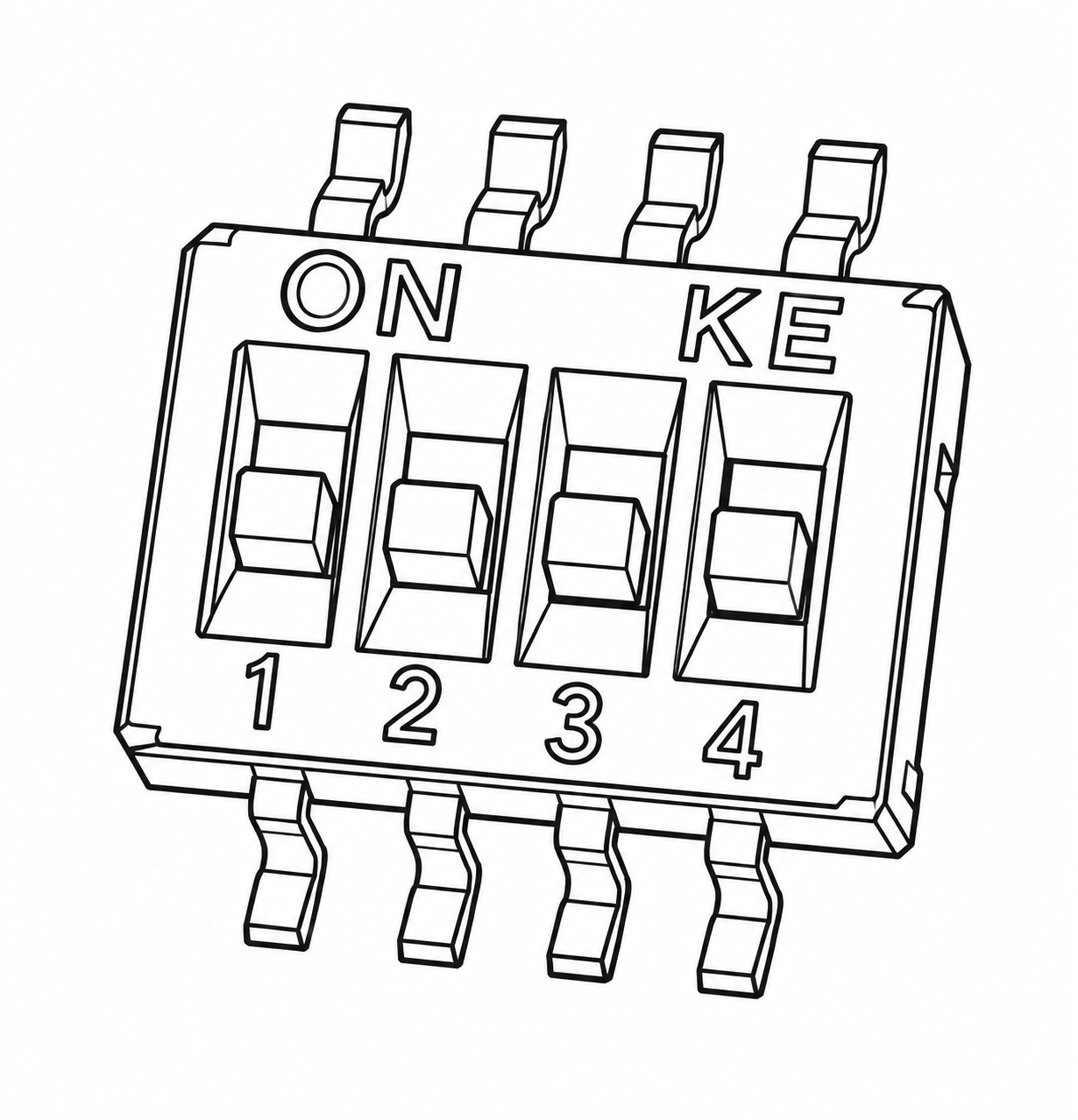
Table 19.1 - SW1 Boot Mode Configuration
Power
The power input voltage of the BZ11 development board is +9V to +36V. On the board, the LM5176 buck-boost converter converts it to +12V, which is then converted by five DC/DC converters into +5V, QSFP_3.3V, +1.8V and FMC_VADJ. The power design of the board is shown below:
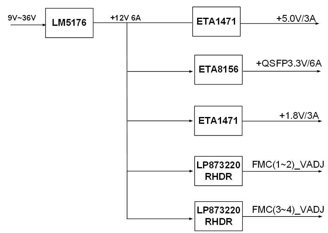
Figure 20.1 - Power Interface in the Schematic
In addition, a PMIC chip TPS6508640 on the board generates all the other power supplies required by the XCZU11EG. For the TPS6508640 power design, please refer to the power chip manual. The design block diagram is as follows:
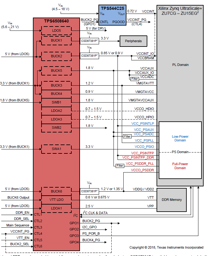
Figure 20.2 - Power Design Block Diagram
The functions assigned to each power rail are shown in the table below:
| Power | Function |
| +5.0V | USB power supply |
| +1.8V | Ethernet and USB power supply |
| QSFP_+3.3V | QSFP power supply |
| FMC_VADJ | FMC and FPGA chip BANK voltage |
Table 20.1 - Power Rail Function Assignment
Fan
Because the ZU11EG generates a large amount of heat during normal operation, we have added a heatsink and a fan on the board for the chip to prevent overheating. The fan is controlled by the Zynq chip, with the control pin connected to the IO of BANK65 (PIN AM20). If the IO level is low, the MOSFET turns on and the fan works; if the IO level is high, the fan stops.
The fan is fixed to the development board with screws before shipment. The fan power is connected to the J11 socket, with red as the positive terminal and black as the negative terminal.
Mechanical Dimensions
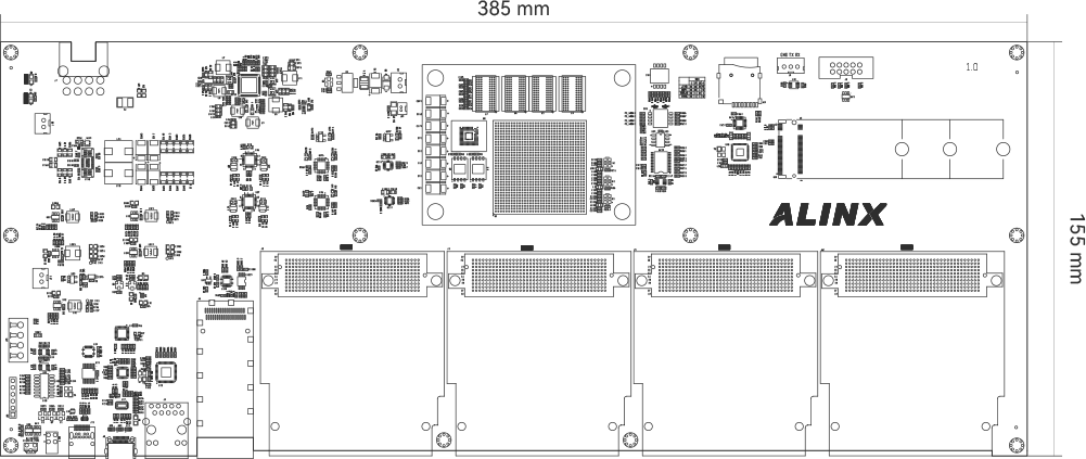
Figure 22.1 - Front View (Top View)
Appendix: List of Abbreviations
| Abbreviation | Full English Name | Description |
| PS | Processor System | The processing subsystem in an SoC, typically including CPU cores, memory controllers, and peripheral interfaces. |
| PL | Programmable Logic | User-configurable FPGA logic resources for implementing custom digital circuits and hardware acceleration. |
| SoC | System on Chip | An integrated circuit combining processors, memory controllers, and peripheral interfaces on a single chip. |
| DDR4 | Double Data Rate 4 SDRAM | Fourth-generation synchronous dynamic memory technology transferring data on both clock edges. |
| eMMC | Embedded Multi Media Card | An embedded non-volatile storage device integrating NAND Flash and a controller in one package. |
| QSPI | Quad Serial Peripheral Interface | A high-speed serial interface using four data lines, commonly used for NOR Flash boot devices. |
| GTH | Gigabit Transceiver | High-speed serial transceivers in Xilinx FPGAs supporting multi-gigabit data rates. |
| UART | Universal Asynchronous Receiver/Transmitter | An asynchronous serial communication interface using TX and RX lines. |
| DP | DisplayPort | A digital display interface standard for video and audio transmission. |
| PCIe | Peripheral Component Interconnect Express | A high-speed serial expansion bus standard. |
| USB | Universal Serial Bus | A standard serial interface for data communication and power delivery. |
| JTAG | Joint Test Action Group | A standardized interface for device testing, boundary scan, and FPGA programming. |
| QSFP+ | Quad Small Form-factor Pluggable Plus | A high-density hot-pluggable optical transceiver supporting up to 40Gbps. |
| MIO | Multiplexed I/O | Multiplexed processor I/O pins configurable as UART, I2C, SPI, or GPIO. |
| PHY | Physical Layer Transceiver | An analog front-end device that converts digital data to/from physical network signals. |
| I2C | Inter-Integrated Circuit | A two-wire serial bus using SDA and SCL for connecting peripherals. |
| RGMII | Reduced Gigabit Media Independent Interface | A reduced-pin-count Ethernet MAC-to-PHY interface supporting up to 1000Mbps. |
| FMC | FPGA Mezzanine Card | A standard mezzanine connector for FPGA I/O expansion. |
| LED | Light Emitting Diode | A semiconductor device that emits light, used for status indication. |
| CANFD | Controller Area Network Flexible Data Rate | An upgraded CAN bus standard supporting flexible data rates up to 5Mbps. |
| GPS | Global Positioning System | A satellite-based navigation system providing location and time synchronization. |
| EEPROM | Electrically Erasable Programmable Read-Only Memory | A non-volatile memory that can be erased and rewritten electrically. |
| DDR | Double Data Rate | Memory technology transferring data on both rising and falling clock edges. |
| PMIC | Power Management IC | A chip that integrates multiple power conversion and management functions. |
Contact information
Alinx Electronic Limited
Company Website: www.en.alinx.com
Service Hotline: +86 21 67676997
Technical Support:technical@alinx.com