
Appearance
HEA19 User Manual

Alinx Electronic Limited
Company Website: www.en.alinx.com
Service Hotline: +86 21 67676997
Technical Support : technical@alinx.com
Document Information
| Item | Description |
| Document Name | Product Manual |
| Product Model | HEA19 |
| Document Version | V1.0 |
| Prepared by | Alinx Electronic Limited |
| Release Date | 2026.11.5 |
Revision History
| Version | Date | Chapter | Revision Summary |
| V1.0 | 2026.11.5 | All | Initial release |
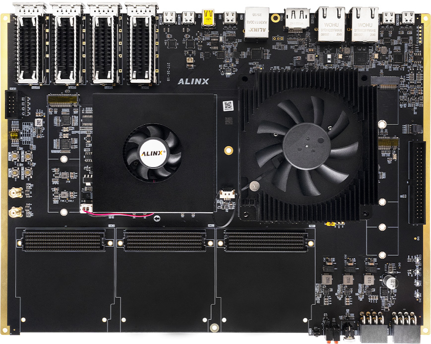
Alinx Electronic Limited is proud to announce the 2026 release of the HEA19 development platform based on XILINX MPSoC and integrated NVIDIA Jetson AGX/THOR modules. This user manual is provided to help you quickly understand the platform.
The development board consists of a Zynq UltraScale+ MPSoC SOM (System-on-Module), an NVIDIA Jetson AGX/THOR module, and a carrier board. The MPSoC SOM and the NVIDIA Jetson AGX/THOR module are interconnected via PCIe Gen3 x8 signals.
The MPSoC SOM features the Xilinx Zynq UltraScale+ MPSoC series ZU19EG FPGA as the main chip. It integrates a quad-core ARM Cortex-A53 processor with FPGA programmable logic on a single chip using Processing System (PS) + Programmable Logic (PL) architecture. The SOM also includes 9 DDR4 SDRAM chips (1GB each), one 32GB eMMC memory chip, and two 512Mb QSPI FLASH chips.
The NVIDIA Jetson AGX/THOR series modules are high-performance, low-power embedded AI computing platforms designed for autonomous machines, robotics, and edge AI applications. They integrate GPU, CPU, high-speed memory, and rich peripheral interfaces into a compact module, enabling complex AI and vision algorithms to run directly on the device in real time.
The board design provides users with a rich set of peripheral interfaces. On the MPSoC side: 4x QSFP 100G fiber optic interfaces, 1x USB3.0 Type-C interface, 1x UART interface each for PS and PL, 1x Gigabit Ethernet interface, 3x FMC HPC interfaces, 1x Mini DP interface, 1x M.2 interface, and 1x TF card slot. On the NVIDIA AGX side: 1x 10G Ethernet interface, 2x USB3.2 Type-C interfaces, 1x M.2 SSD interface, and 1x M.2 WiFi/BT interface.
The MPSoC and NVIDIA AGX/THOR are interconnected via 8 high-speed GT lanes with a throughput of 80Gbps, enhancing the data interaction and processing capability of the MPSoC.
Chapter 1 Overview
This chapter provides a brief functional introduction to the HEA19 development platform.
The development board is mainly composed of the MPSoC ZU19EG system and the NVIDIA ORIN AGX/THOR module. Data transmission and communication between the MPSoC and ORIN AGX/THOR module are via PCIe 3.0 x8. The following diagram shows the overall architecture of the development system:
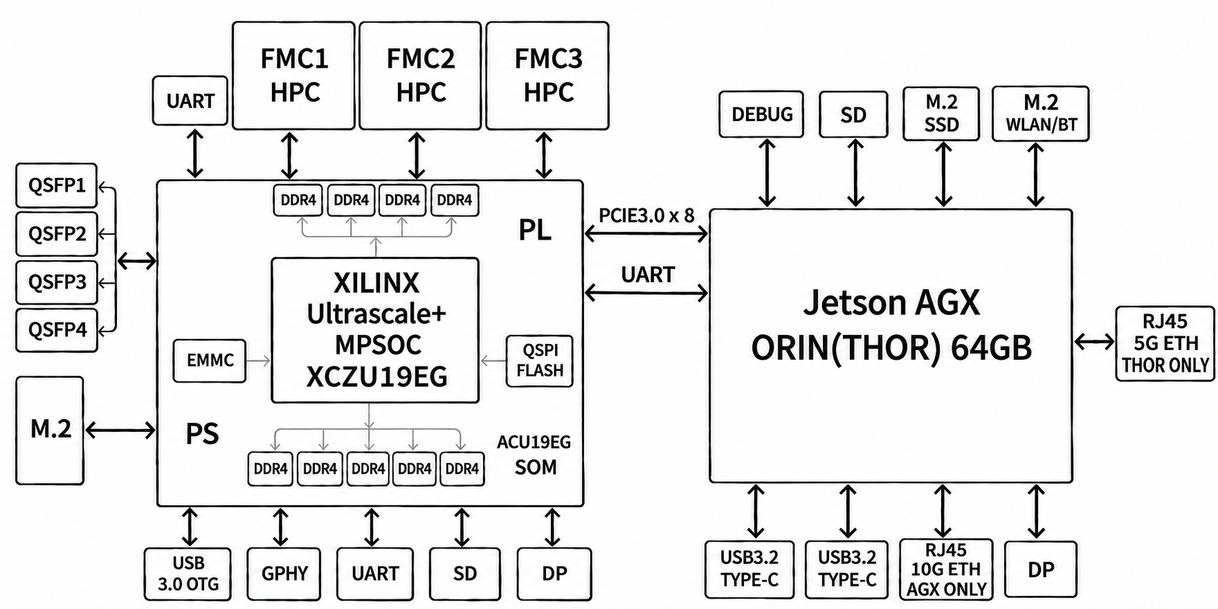
This diagram illustrates the interfaces and features of the development platform.
ZU19EG SOM: Composed of ZU19EG + 5GB ECC DDR4 (PS) + 4GB DDR4 (PL) + 32GB eMMC FLASH + 128MB QSPI FLASH. Two crystal oscillators provide clocks: a single-ended 33.3333MHz oscillator for the PS system, and a differential 200MHz oscillator for the PL logic DDR reference clock.
NVIDIA ORIN AGX/THOR Module: The NVIDIA Jetson AGX/THOR series is a System-on-Module (SoM) for high-performance embedded AI and edge computing. It integrates GPU, CPU, memory, storage controller, and high-speed I/O on a compact PCB, with peripheral expansion via a carrier board. The AGX module supports up to 275 TOPS of AI compute, and the THOR module supports 2070 TOPS. The module dimensions are 100mm x 87mm x 16mm, connected to the carrier board via a 699-pin board-to-board connector.
MPSoC Peripheral Interfaces
M.2 Interface: 1x PCIe x1 standard M.2 interface for connecting M.2 SSD solid-state drives, with a data transfer rate up to 5Gbps.
DP Output Interface: 1x mini DisplayPort output interface for video display. Supports up to 4K@30Hz or 1080P@60Hz output.
USB3.0 Type-C Interface: 1x USB3.0 OTG interface with Type-C connector. Supports HOST, SLAVE, and OTG modes.
Gigabit Ethernet Interface: 1x 10M/100M/1000M Ethernet RJ45 interface for Ethernet data exchange with computers or other network devices.
Micro SD Card Slot: 1x Micro SD card slot for storing OS images and file systems.
FMC Expansion Ports: 3 standard FMC HPC expansion ports. FMC1 and FMC2 support various XILINX or ALINX FMC modules (HDMI input/output modules, dual-camera modules, high-speed AD modules, etc.). FMC3 operates at 3.3V and can be used with our FPGA expansion IO module (FL1010V).
UART Interface: 2x UART-to-USB interfaces, one for PS and one for PL. The PS interface uses a Type-C connector, and the PL interface uses a 3-pin header, for FPGA program debugging.
4x QSFP28 Fiber Optic Interfaces: 4 GTY transceivers connected to QSFP28 interfaces. Each lane supports 25Gbps, for an aggregate data rate of 100Gbps per port.
JTAG Interface: 1x 10-pin 2.54mm standard JTAG port. Users can debug and download the ZU19EG system using a XILINX download cable.
LED Indicators: 3 user LEDs, 1 power LED, and 1 DONE configuration LED on the MPSoC side.
Buttons: 3 buttons on the MPSoC side: POWER-SW and two user buttons.
ORIN AGX/THOR Peripheral Interfaces
USB3.2 Interface: 2x USB3.2 Type-C interfaces, supporting HOST, OTG, and SLAVE modes.
10G Ethernet Interface (AGX only): 1x 10G Ethernet RJ45 interface for ORIN AGX data exchange with computers or other network devices.
5G Ethernet Interface (THOR only): 1x 5G Ethernet RJ45 interface for ORIN THOR module data exchange with computers or other network devices.
DP Output Interface: 1x standard DisplayPort output interface for video display. Supports up to 4K@30Hz or 1080P@60Hz output.
M.2 SSD Interface: 1x M.2 KEY-M interface for connecting NVMe SSD solid-state drives, with a data transfer rate up to 5Gbps.
M.2 WiFi/BT Interface: 1x M.2 KEY-E interface for connecting WiFi/BT modules, with a data transfer rate up to 5Gbps.
UART Interface: 1x UART-to-USB interface via a Type-C connector, for ORIN AGX program debugging.
Buttons: 2 buttons on the ORIN AGX side: system reset button (SYS_RESET) and recovery button (FORCE_RECOVERY).
LED Indicator: 1 user LED on the ORIN AGX/THOR side.
PCIe Communication: The MPSoC connects to the Jetson Orin AGX/THOR module via PCIe x8 for PCIe data communication. Supports PCI Express 3.0 standard, with a per-lane data rate up to 8Gbps.
Chapter 2 MPSoC System
2.1 MPSoC SOM
The ACU19EG SOM features the XILINX Zynq UltraScale+ MPSoC EG series XCZU19EG-2FFVC1760I chip.
This SOM uses 9 Micron MT40A512M16LY DDR4 chips. The PS side has 5 DDR4 chips forming a 72-bit data bus width (with ECC support). The PL side has 4 DDR4 chips forming a 64-bit data bus width. Each DDR4 chip has a capacity of 1GB, and the DDR4 SDRAM operates at up to 1200MHz (2400Mbps data rate). The SOM also integrates 2x 512Mbit QSPI FLASH chips and a 32GB eMMC FLASH chip for boot storage configuration and system files.
To connect to the carrier board, this SOM uses 8x 120-pin board-to-board connectors that expand the PS-side USB2.0 interface, Gigabit Ethernet interface, SD card interface, and other remaining MIO ports. It also expands 4 pairs of PS MGT high-speed transceiver interfaces, as well as 48 PL-side GTH/GTY transceivers and almost all IO ports (HP I/O: 240, HD I/O: 96). The traces between the XCZU19EG chip and the connectors are length-matched and differential-routed. The SOM dimensions are only 80*80mm, making it ideal for secondary development.
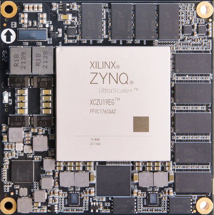
Figure 2.1.1 - ACU19EG SOM Top View
2.1.1 ZYNQ Chip
The development board uses the Xilinx Zynq UltraScale+ MPSoCs EG series chip, model XCZU19EG-2FFVC1760I. The ZU19EG PS system integrates 4 ARM Cortex™-A53 processors up to 1.3GHz with 2-level cache. The ZU19EG also includes 2 Cortex-R5 processors up to 533MHz.
The ZU19EG chip supports 32-bit or 64-bit DDR4, LPDDR4, DDR3, DDR3L, and LPDDR3 memory devices. The PS side provides a rich set of high-speed interfaces such as PCIe Gen2, USB3.0, SATA 3.1, and DisplayPort, as well as USB2.0, Gigabit Ethernet, SD/SDIO, I2C, CAN, UART, and GPIO interfaces. The PL side contains rich programmable logic cells, DSP slices, and internal RAM. The overall block diagram of the ZU19EG chip is shown below.
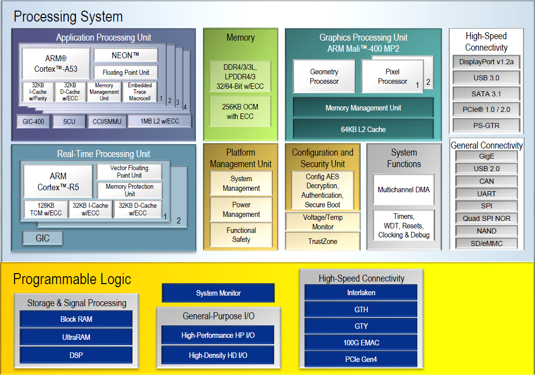
Figure 2.1.1.1 - ZYNQ ZU19EG Chip Block Diagram
Key parameters of the PS system:
Quad-core ARM Cortex™-A53 processor up to 1.3GHz, 32KB L1 instruction and data cache per CPU, 1MB L2 cache shared by 2 CPUs.
Dual-core ARM Cortex-R5 processor up to 533MHz, 32KB L1 instruction and data cache per CPU, and 128K tightly coupled memory.
External memory interface: supports 32/64-bit DDR4/3/3L, LPDDR4/3 interfaces.
Static memory interface: supports NAND, 2x Quad-SPI FLASH.
High-speed connectivity: PCIe Gen2 x4, 2x USB3.0, SATA 3.1, DisplayPort, 4x Tri-mode Gigabit Ethernet.
General connectivity: 2x USB2.0, 2x SD/SDIO, 2x UART, 2x CAN 2.0B, 2x I2C, 2x SPI, 4x 32-bit GPIO.
Power management: supports Full/Low/PL/Battery four-domain power partitioning.
Cryptography: supports RSA, AES, and SHA.
System monitoring: 10-bit 1Mbps ADC for temperature and voltage monitoring.
Key parameters of the PL logic:
System Logic Cells: 1143K;
CLB Flip-Flops: 1045K;
CLB LUTs: 523K;
Block RAM: 34.6Mb;
Clock Management Tiles (CMTs): 11
DSP Slices: 1968
GTH 16.3 Gb/s transceivers: 32
GTY 28.21 Gb/s transceivers: 16
The XCZU19EG-2FFVC1760I chip has a -2 speed grade, industrial grade, in FFVC1760 package.
2.1.2 DDR4 DRAM
The ACU19EG SOM is equipped with 9 Micron 1GB DDR4 chips, model MT40A512M16LY-062E. The PS side has 5 DDR4 chips forming a 72-bit data bus width (with ECC support), each with 1GB capacity. The PL side has 4 DDR4 chips forming a 64-bit data bus width, each with 1GB capacity. The PS-side DDR4 SDRAM operates at up to 1200MHz (2400Mbps data rate), with 5 DDR4 chips connected directly to the PS BANK 504 memory interface. The PL-side DDR4 SDRAM operates at up to 1200MHz (2400Mbps data rate), with 4 DDR4 chips connected to the FPGA BANK 69, 70, 71 interfaces. The detailed configuration of PS-side and PL-side DDR4 SDRAM is shown in the table below.
| Location | Designator | Chip Model | Capacity | Manufacturer |
| PS | U4,U5,U6,U7,U162 | MT40A512M16LY-062E | 512M x 16bit | Micron |
| PL | U18,U19,U20,U21 | MT40A512M16LY-062E | 512M x 16bit | Micron |
Table 2.1.2.1 - DDR4 SDRAM Configuration
DDR4 hardware design requires careful consideration of signal integrity. We have fully accounted for matching/termination resistors, trace impedance control, and length matching in the circuit and PCB design to ensure high-speed and stable DDR4 operation. The PS-side DDR4 hardware connection is shown in the figure.
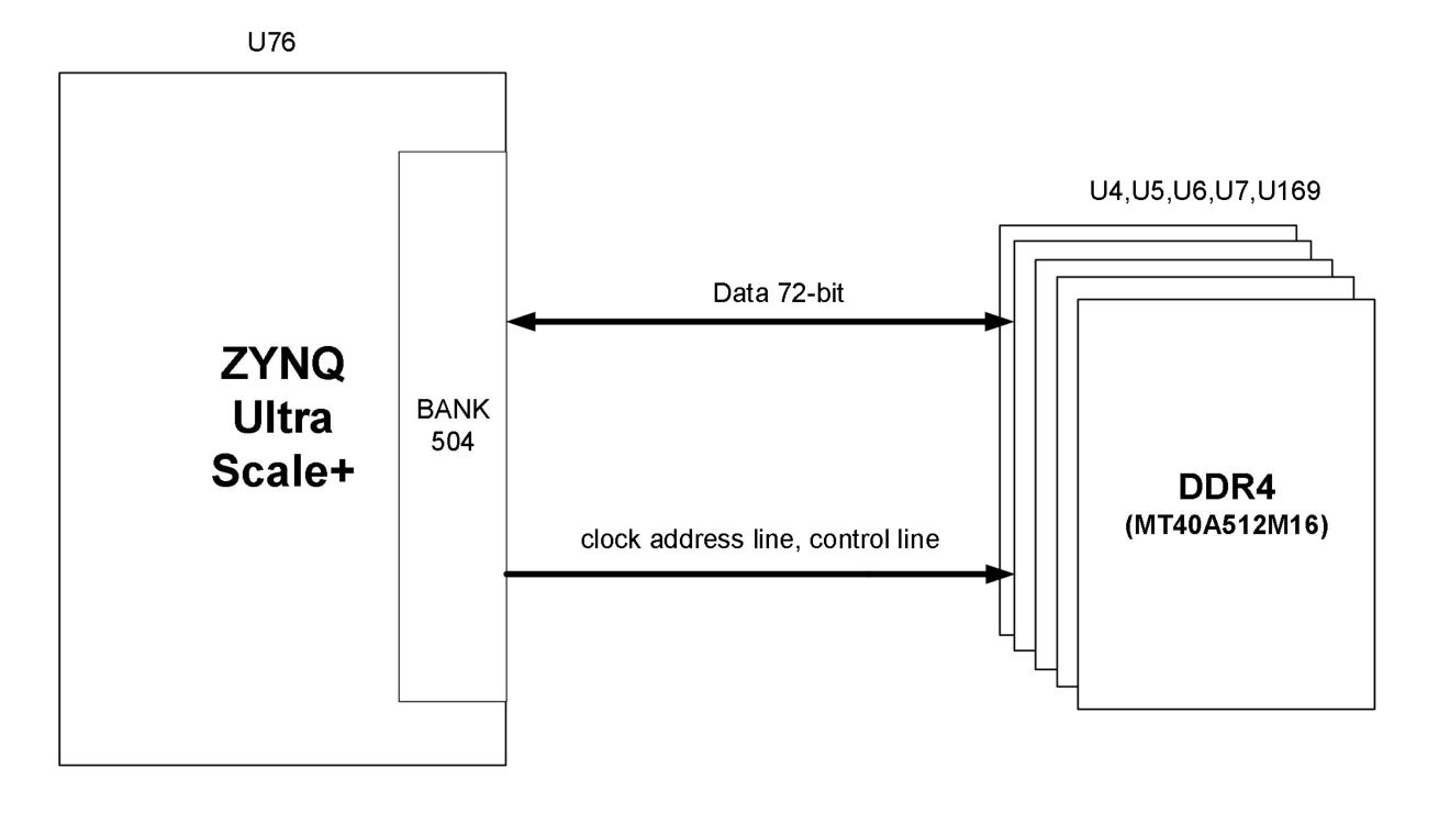
Figure 2.1.2.1 - PS-side DDR4 DRAM Schematic
The PL-side DDR4 DRAM hardware connection is shown in the figure below.
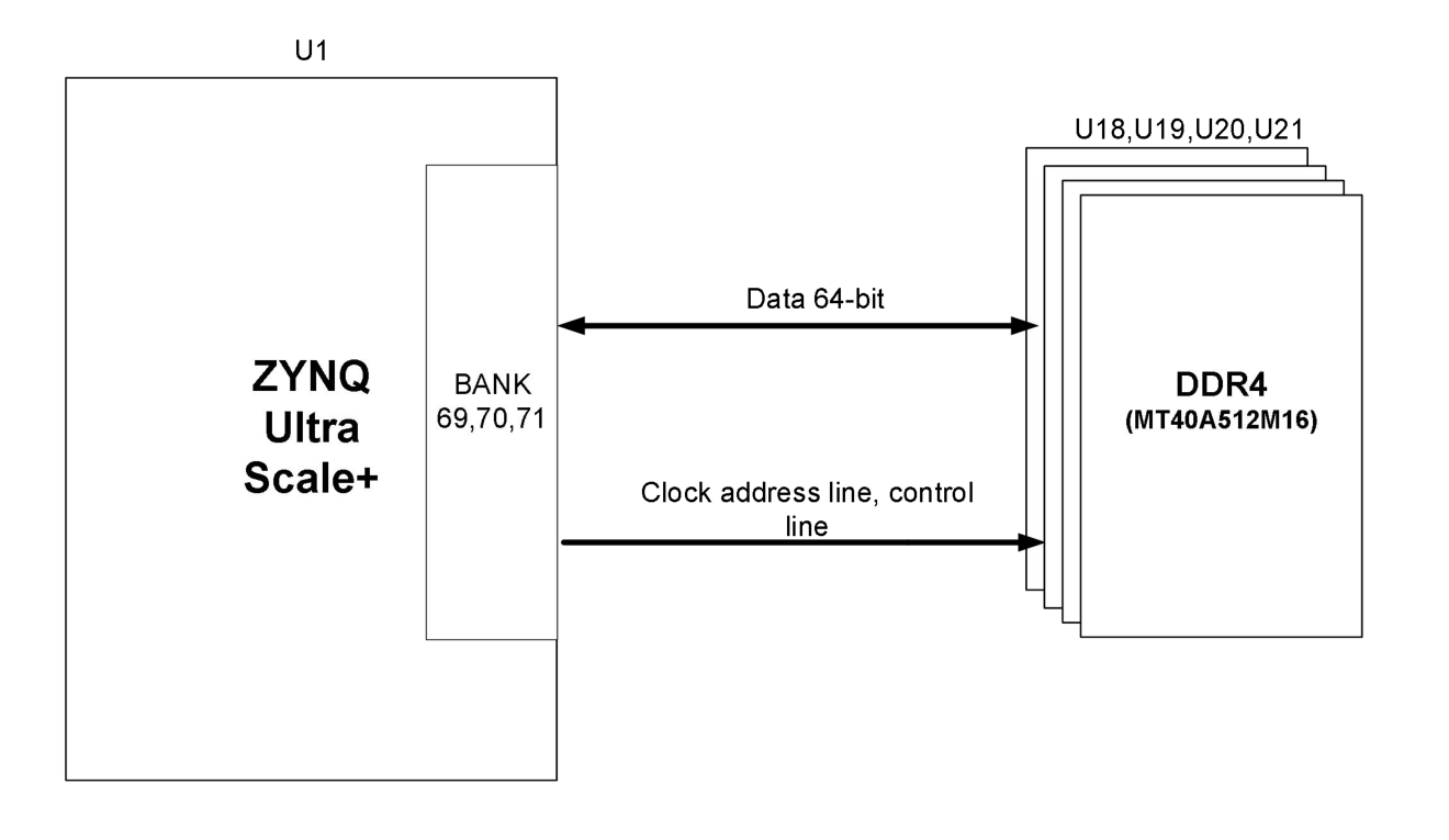
Figure 2.1.2.2 - PL-side DDR4 DRAM Schematic
PS-side DDR4 SDRAM Pin Assignment:
| Signal Name | Pin Name | Pin Number |
| PS_DDR4_DQS0_N | PS_DDR_DQS_N0_504 | BA30 |
| PS_DDR4_DQS0_P | PS_DDR_DQS_P0_504 | AY30 |
| PS_DDR4_DQS1_N | PS_DDR_DQS_N1_504 | AY33 |
| PS_DDR4_DQS1_P | PS_DDR_DQS_P1_504 | AY32 |
| PS_DDR4_DQS2_N | PS_DDR_DQS_N2_504 | AT30 |
| PS_DDR4_DQS2_P | PS_DDR_DQS_P2_504 | AR30 |
| PS_DDR4_DQS3_N | PS_DDR_DQS_N3_504 | AT32 |
| PS_DDR4_DQS3_P | PS_DDR_DQS_P3_504 | AR32 |
| PS_DDR4_DQS4_N | PS_DDR_DQS_N4_504 | AR40 |
| PS_DDR4_DQS4_P | PS_DDR_DQS_P4_504 | AP40 |
| PS_DDR4_DQS5_N | PS_DDR_DQS_N5_504 | AK37 |
| PS_DDR4_DQS5_P | PS_DDR_DQS_P5_504 | AJ37 |
| PS_DDR4_DQS6_N | PS_DDR_DQS_N6_504 | AU41 |
| PS_DDR4_DQS6_P | PS_DDR_DQS_P6_504 | AU40 |
| PS_DDR4_DQS7_N | PS_DDR_DQS_N7_504 | AL41 |
| PS_DDR4_DQS7_P | PS_DDR_DQS_P7_504 | AL40 |
| PS_DDR4_DQS8_N | PS_DDR_DQS_N8_504 | AY40 |
| PS_DDR4_DQS8_P | PS_DDR_DQS_P8_504 | AY39 |
| PS_DDR4_DQ0 | PS_DDR_DQ0_504 | AV29 |
| PS_DDR4_DQ1 | PS_DDR_DQ1_504 | AW30 |
| PS_DDR4_DQ2 | PS_DDR_DQ2_504 | AW29 |
| PS_DDR4_DQ3 | PS_DDR_DQ3_504 | AW31 |
| PS_DDR4_DQ4 | PS_DDR_DQ4_504 | BB31 |
| PS_DDR4_DQ5 | PS_DDR_DQ5_504 | BB30 |
| PS_DDR4_DQ6 | PS_DDR_DQ6_504 | BB29 |
| PS_DDR4_DQ7 | PS_DDR_DQ7_504 | BA31 |
| PS_DDR4_DQ8 | PS_DDR_DQ8_504 | BB33 |
| PS_DDR4_DQ9 | PS_DDR_DQ9_504 | BA32 |
| PS_DDR4_DQ10 | PS_DDR_DQ10_504 | BA33 |
| PS_DDR4_DQ11 | PS_DDR_DQ11_504 | BB34 |
| PS_DDR4_DQ12 | PS_DDR_DQ12_504 | AV31 |
| PS_DDR4_DQ13 | PS_DDR_DQ13_504 | AW32 |
| PS_DDR4_DQ14 | PS_DDR_DQ14_504 | AV32 |
| PS_DDR4_DQ15 | PS_DDR_DQ15_504 | AV33 |
| PS_DDR4_DQ16 | PS_DDR_DQ16_504 | AN29 |
| PS_DDR4_DQ17 | PS_DDR_DQ17_504 | AP29 |
| PS_DDR4_DQ18 | PS_DDR_DQ18_504 | AP30 |
| PS_DDR4_DQ19 | PS_DDR_DQ19_504 | AP31 |
| PS_DDR4_DQ20 | PS_DDR_DQ20_504 | AT31 |
| PS_DDR4_DQ21 | PS_DDR_DQ21_504 | AU30 |
| PS_DDR4_DQ22 | PS_DDR_DQ22_504 | AU31 |
| PS_DDR4_DQ23 | PS_DDR_DQ23_504 | AU29 |
| PS_DDR4_DQ24 | PS_DDR_DQ24_504 | AV34 |
| PS_DDR4_DQ25 | PS_DDR_DQ25_504 | AU33 |
| PS_DDR4_DQ26 | PS_DDR_DQ26_504 | AT33 |
| PS_DDR4_DQ27 | PS_DDR_DQ27_504 | AU34 |
| PS_DDR4_DQ28 | PS_DDR_DQ28_504 | AN33 |
| PS_DDR4_DQ29 | PS_DDR_DQ29_504 | AP32 |
| PS_DDR4_DQ30 | PS_DDR_DQ30_504 | AN32 |
| PS_DDR4_DQ31 | PS_DDR_DQ31_504 | AN31 |
| PS_DDR4_DQ32 | PS_DDR_DQ32_504 | AN41 |
| PS_DDR4_DQ33 | PS_DDR_DQ33_504 | AN42 |
| PS_DDR4_DQ34 | PS_DDR_DQ34_504 | AP42 |
| PS_DDR4_DQ35 | PS_DDR_DQ35_504 | AP41 |
| PS_DDR4_DQ36 | PS_DDR_DQ36_504 | AN39 |
| PS_DDR4_DQ37 | PS_DDR_DQ37_504 | AR38 |
| PS_DDR4_DQ38 | PS_DDR_DQ38_504 | AP39 |
| PS_DDR4_DQ39 | PS_DDR_DQ39_504 | AN38 |
| PS_DDR4_DQ40 | PS_DDR_DQ40_504 | AL37 |
| PS_DDR4_DQ41 | PS_DDR_DQ41_504 | AL38 |
| PS_DDR4_DQ42 | PS_DDR_DQ42_504 | AK38 |
| PS_DDR4_DQ43 | PS_DDR_DQ43_504 | AK39 |
| PS_DDR4_DQ44 | PS_DDR_DQ44_504 | AJ36 |
| PS_DDR4_DQ45 | PS_DDR_DQ45_504 | AL35 |
| PS_DDR4_DQ46 | PS_DDR_DQ46_504 | AJ35 |
| PS_DDR4_DQ47 | PS_DDR_DQ47_504 | AK35 |
| PS_DDR4_DQ48 | PS_DDR_DQ48_504 | AR42 |
| PS_DDR4_DQ49 | PS_DDR_DQ49_504 | AT41 |
| PS_DDR4_DQ50 | PS_DDR_DQ50_504 | AT42 |
| PS_DDR4_DQ51 | PS_DDR_DQ51_504 | AT40 |
| PS_DDR4_DQ52 | PS_DDR_DQ52_504 | AV42 |
| PS_DDR4_DQ53 | PS_DDR_DQ53_504 | AV41 |
| PS_DDR4_DQ54 | PS_DDR_DQ54_504 | AV39 |
| PS_DDR4_DQ55 | PS_DDR_DQ55_504 | AV38 |
| PS_DDR4_DQ56 | PS_DDR_DQ56_504 | AM39 |
| PS_DDR4_DQ57 | PS_DDR_DQ57_504 | AM38 |
| PS_DDR4_DQ58 | PS_DDR_DQ58_504 | AM40 |
| PS_DDR4_DQ59 | PS_DDR_DQ59_504 | AM41 |
| PS_DDR4_DQ60 | PS_DDR_DQ60_504 | AJ42 |
| PS_DDR4_DQ61 | PS_DDR_DQ61_504 | AK42 |
| PS_DDR4_DQ62 | PS_DDR_DQ62_504 | AK40 |
| PS_DDR4_DQ63 | PS_DDR_DQ63_504 | AK41 |
| PS_DDR4_DQ64 | PS_DDR4_DQ64_504 | BB40 |
| PS_DDR4_DQ65 | PS_DDR4_DQ65_504 | BA41 |
| PS_DDR4_DQ66 | PS_DDR4_DQ66_504 | BA42 |
| PS_DDR4_DQ67 | PS_DDR4_DQ67_504 | BA40 |
| PS_DDR4_DQ68 | PS_DDR4_DQ68_504 | AW42 |
| PS_DDR4_DQ69 | PS_DDR4_DQ69_504 | AW40 |
| PS_DDR4_DQ70 | PS_DDR4_DQ70_504 | AW41 |
| PS_DDR4_DQ71 | PS_DDR4_DQ71_504 | AW39 |
| PS_DDR4_DM0 | PS_DDR_DM0_504 | AY29 |
| PS_DDR4_DM1 | PS_DDR_DM1_504 | AY34 |
| PS_DDR4_DM2 | PS_DDR_DM2_504 | AR29 |
| PS_DDR4_DM3 | PS_DDR_DM3_504 | AR33 |
| PS_DDR4_DM4 | PS_DDR_DM4_504 | AR39 |
| PS_DDR4_DM5 | PS_DDR_DM5_504 | AL36 |
| PS_DDR4_DM6 | PS_DDR_DM6_504 | AU39 |
| PS_DDR4_DM7 | PS_DDR_DM7_504 | AL42 |
| PS_DDR4_DM8 | PS_DDR_DM8_504 | AY42 |
| PS_DDR4_A0 | PS_DDR_A0_504 | BA38 |
| PS_DDR4_A1 | PS_DDR_A1_504 | BB36 |
| PS_DDR4_A2 | PS_DDR_A2_504 | BA35 |
| PS_DDR4_A3 | PS_DDR_A3_504 | BB35 |
| PS_DDR4_A4 | PS_DDR_A4_504 | BB38 |
| PS_DDR4_A5 | PS_DDR_A5_504 | AY35 |
| PS_DDR4_A6 | PS_DDR_A6_504 | AP37 |
| PS_DDR4_A7 | PS_DDR_A7_504 | AT36 |
| PS_DDR4_A8 | PS_DDR_A8_504 | AR35 |
| PS_DDR4_A9 | PS_DDR_A9_504 | AT35 |
| PS_DDR4_A10 | PS_DDR_A10_504 | AU35 |
| PS_DDR4_A11 | PS_DDR_A11_504 | AU36 |
| PS_DDR4_A12 | PS_DDR_A12_504 | AW36 |
| PS_DDR4_A13 | PS_DDR_A13_504 | AW37 |
| PS_DDR4_ACT_B | PS_DDR_ACT_N_504 | AR37 |
| PS_DDR4_ALERT_B | PS_DDR_ALERT_N_504 | AM36 |
| PS_DDR4_BA0 | PS_DDR_BA0_504 | AN37 |
| PS_DDR4_BA1 | PS_DDR_BA1_504 | AN36 |
| PS_DDR4_BG0 | PS_DDR_BG0_504 | AP36 |
| PS_DDR4_CAS_B | PS_DDR_A15_504 | AW34 |
| PS_DDR4_CKE0 | PS_DDR_CKE0_504 | AY38 |
| PS_DDR4_CLK0_N | PS_DDR_CK_N0_504 | BA37 |
| PS_DDR4_CLK0_P | PS_DDR_CK0_504 | BA36 |
| PS_DDR4_CS0_B | PS_DDR_CS_N0_504 | AY37 |
| PS_DDR4_ODT0 | PS_DDR_ODT0_504 | BB39 |
| PS_DDR4_PARITY | PS_DDR_PARITY_504 | AM35 |
| PS_DDR4_RAS_B | PS_DDR_A16_504 | AR34 |
| PS_DDR4_RESET_B | PS_DDR_RAM_RST_N_504 | AM34 |
| PS_DDR4_WE_B | PS_DDR_A14_504 | AW35 |
Table 2.1.2.2 - PS-side DDR4 SDRAM Pin Assignment
PL-side DDR4 SDRAM Pin Assignment:
| Signal Name | Pin Name | Pin Number |
| PL_DDR4_DQS0_N | IO_L10N_T1U_N7_QBC_AD4N_70 | G23 |
| PL_DDR4_DQS0_P | IO_L10P_T1U_N6_QBC_AD4P_70 | H23 |
| PL_DDR4_DQS1_N | IO_L4N_T0U_N7_DBC_AD7N_70 | K24 |
| PL_DDR4_DQS1_P | IO_L4P_T0U_N6_DBC_AD7P_70 | L24 |
| PL_DDR4_DQS2_N | IO_L22N_T3U_N7_DBC_AD0N_70 | B26 |
| PL_DDR4_DQS2_P | IO_L22P_T3U_N6_DBC_AD0P_70 | B25 |
| PL_DDR4_DQS3_N | IO_L16N_T2U_N7_QBC_AD3N_70 | E27 |
| PL_DDR4_DQS3_P | IO_L16P_T2U_N6_QBC_AD3P_70 | E26 |
| PL_DDR4_DQS4_N | IO_L10N_T1U_N7_QBC_AD4N_69 | A32 |
| PL_DDR4_DQS4_P | IO_L10P_T1U_N6_QBC_AD4P_69 | B31 |
| PL_DDR4_DQS5_N | IO_L4N_T0U_N7_DBC_AD7N_69 | F30 |
| PL_DDR4_DQS5_P | IO_L4P_T0U_N6_DBC_AD7P_69 | G30 |
| PL_DDR4_DQS6_N | IO_L22N_T3U_N7_DBC_AD0N_69 | A40 |
| PL_DDR4_DQS6_P | IO_L22P_T3U_N6_DBC_AD0P_69 | A39 |
| PL_DDR4_DQS7_N | IO_L16N_T2U_N7_QBC_AD3N_69 | C34 |
| PL_DDR4_DQS7_P | IO_L16P_T2U_N6_QBC_AD3P_69 | D34 |
| PL_DDR4_DQ0 | IO_L12N_T1U_N11_GC_70 | G25 |
| PL_DDR4_DQ1 | IO_L9N_T1L_N5_AD12N_70 | J24 |
| PL_DDR4_DQ2 | IO_L11P_T1U_N8_GC_70 | H25 |
| PL_DDR4_DQ3 | IO_L8N_T1L_N3_AD5N_70 | J26 |
| PL_DDR4_DQ4 | IO_L12P_T1U_N10_GC_70 | H24 |
| PL_DDR4_DQ5 | IO_L8P_T1L_N2_AD5P_70 | K26 |
| PL_DDR4_DQ6 | IO_L11N_T1U_N9_GC_70 | H26 |
| PL_DDR4_DQ7 | IO_L9P_T1L_N4_AD12P_70 | J23 |
| PL_DDR4_DQ8 | IO_L2P_T0L_N2_70 | M25 |
| PL_DDR4_DQ9 | IO_L6P_T0U_N10_AD6P_70 | M23 |
| PL_DDR4_DQ10 | IO_L2N_T0L_N3_70 | L25 |
| PL_DDR4_DQ11 | IO_L6N_T0U_N11_AD6N_70 | L23 |
| PL_DDR4_DQ12 | IO_L3P_T0L_N4_AD15P_70 | N24 |
| PL_DDR4_DQ13 | IO_L5N_T0U_N9_AD14N_70 | N23 |
| PL_DDR4_DQ14 | IO_L3N_T0L_N5_AD15N_70 | N25 |
| PL_DDR4_DQ15 | IO_L5P_T0U_N8_AD14P_70 | P23 |
| PL_DDR4_DQ16 | IO_L20N_T3L_N3_AD1N_70 | A28 |
| PL_DDR4_DQ17 | IO_L24P_T3U_N10_70 | A24 |
| PL_DDR4_DQ18 | IO_L21N_T3L_N5_AD8N_70 | B27 |
| PL_DDR4_DQ19 | IO_L23N_T3U_N9_70 | C25 |
| PL_DDR4_DQ20 | IO_L20P_T3L_N2_AD1P_70 | A27 |
| PL_DDR4_DQ21 | IO_L21P_T3L_N4_AD8P_70 | C26 |
| PL_DDR4_DQ22 | IO_L24N_T3U_N11_70 | A25 |
| PL_DDR4_DQ23 | IO_L23P_T3U_N8_70 | C24 |
| PL_DDR4_DQ24 | IO_L15P_T2L_N4_AD11P_70 | F27 |
| PL_DDR4_DQ25 | IO_L14P_T2L_N2_GC_70 | F25 |
| PL_DDR4_DQ26 | IO_L17P_T2U_N8_AD10P_70 | D27 |
| PL_DDR4_DQ27 | IO_L14N_T2L_N3_GC_70 | E25 |
| PL_DDR4_DQ28 | IO_L15N_T2L_N5_AD11N_70 | F28 |
| PL_DDR4_DQ29 | IO_L18P_T2U_N10_AD2P_70 | F24 |
| PL_DDR4_DQ30 | IO_L17N_T2U_N9_AD10N_70 | D28 |
| PL_DDR4_DQ31 | IO_L18N_T2U_N11_AD2N_70 | E24 |
| PL_DDR4_DQ32 | IO_L11N_T1U_N9_GC_69 | D31 |
| PL_DDR4_DQ33 | IO_L9P_T1L_N4_AD12P_69 | A29 |
| PL_DDR4_DQ34 | IO_L12P_T1U_N10_GC_69 | C30 |
| PL_DDR4_DQ35 | IO_L9N_T1L_N5_AD12N_69 | A30 |
| PL_DDR4_DQ36 | IO_L11P_T1U_N8_GC_69 | E31 |
| PL_DDR4_DQ37 | IO_L8P_T1L_N2_AD5P_69 | C29 |
| PL_DDR4_DQ38 | IO_L12N_T1U_N11_GC_69 | C31 |
| PL_DDR4_DQ39 | IO_L8N_T1L_N3_AD5N_69 | B30 |
| PL_DDR4_DQ40 | IO_L3N_T0L_N5_AD15N_69 | F32 |
| PL_DDR4_DQ41 | IO_L5P_T0U_N8_AD14P_69 | G28 |
| PL_DDR4_DQ42 | IO_L2N_T0L_N3_69 | H30 |
| PL_DDR4_DQ43 | IO_L6P_T0U_N10_AD6P_69 | J28 |
| PL_DDR4_DQ44 | IO_L2P_T0L_N2_69 | J30 |
| PL_DDR4_DQ45 | IO_L6N_T0U_N11_AD6N_69 | H28 |
| PL_DDR4_DQ46 | IO_L3P_T0L_N4_AD15P_69 | F31 |
| PL_DDR4_DQ47 | IO_L5N_T0U_N9_AD14N_69 | F29 |
| PL_DDR4_DQ48 | IO_L24P_T3U_N10_69 | C42 |
| PL_DDR4_DQ49 | IO_L21N_T3L_N5_AD8N_69 | A38 |
| PL_DDR4_DQ50 | IO_L23P_T3U_N8_69 | B40 |
| PL_DDR4_DQ51 | IO_L20N_T3L_N3_AD1N_69 | B37 |
| PL_DDR4_DQ52 | IO_L24N_T3U_N11_69 | B42 |
| PL_DDR4_DQ53 | IO_L20P_T3L_N2_AD1P_69 | B36 |
| PL_DDR4_DQ54 | IO_L23N_T3U_N9_69 | B41 |
| PL_DDR4_DQ55 | IO_L21P_T3L_N4_AD8P_69 | A37 |
| PL_DDR4_DQ56 | IO_L15N_T2L_N5_AD11N_69 | C33 |
| PL_DDR4_DQ57 | IO_L17N_T2U_N9_AD10N_69 | A35 |
| PL_DDR4_DQ58 | IO_L15P_T2L_N4_AD11P_69 | D33 |
| PL_DDR4_DQ59 | IO_L14N_T2L_N3_GC_69 | B33 |
| PL_DDR4_DQ60 | IO_L14P_T2L_N2_GC_69 | B32 |
| PL_DDR4_DQ61 | IO_L18N_T2U_N11_AD2N_69 | A34 |
| PL_DDR4_DQ62 | IO_L17P_T2U_N8_AD10P_69 | B35 |
| PL_DDR4_DQ63 | IO_L18P_T2U_N10_AD2P_69 | A33 |
| PL_DDR4_DM0 | IO_L7P_T1L_N0_QBC_AD13P_70 | K27 |
| PL_DDR4_DM1 | IO_L1P_T0L_N0_DBC_70 | P26 |
| PL_DDR4_DM2 | IO_L19P_T3L_N0_DBC_AD9P_70 | C28 |
| PL_DDR4_DM3 | IO_L13P_T2L_N0_GC_QBC_70 | G26 |
| PL_DDR4_DM4 | IO_L7P_T1L_N0_QBC_AD13P_69 | E29 |
| PL_DDR4_DM5 | IO_L1P_T0L_N0_DBC_69 | K29 |
| PL_DDR4_DM6 | IO_L19P_T3L_N0_DBC_AD9P_69 | C36 |
| PL_DDR4_DM7 | IO_L13P_T2L_N0_GC_QBC_69 | E32 |
| PL_DDR4_A0 | IO_L6N_T0U_N11_AD6N_71 | M21 |
| PL_DDR4_A1 | IO_L5N_T0U_N9_AD14N_71 | N21 |
| PL_DDR4_A2 | IO_L16N_T2U_N7_QBC_AD3N_71 | E20 |
| PL_DDR4_A3 | IO_L5P_T0U_N8_AD14P_71 | P21 |
| PL_DDR4_A4 | IO_L17P_T2U_N8_AD10P_71 | E21 |
| PL_DDR4_A5 | IO_L15N_T2L_N5_AD11N_71 | E19 |
| PL_DDR4_A6 | IO_L6P_T0U_N10_AD6P_71 | M22 |
| PL_DDR4_A7 | IO_L7N_T1L_N1_QBC_AD13N_71 | J19 |
| PL_DDR4_A8 | IO_L9N_T1L_N5_AD12N_71 | J21 |
| PL_DDR4_A9 | IO_L16P_T2U_N6_QBC_AD3P_71 | F20 |
| PL_DDR4_A10 | IO_L8P_T1L_N2_AD5P_71 | L20 |
| PL_DDR4_A11 | IO_L3P_T0L_N4_AD15P_71 | M20 |
| PL_DDR4_A12 | IO_L4P_T0U_N6_DBC_AD7P_71 | N20 |
| PL_DDR4_A13 | IO_L7P_T1L_N0_QBC_AD13P_71 | K19 |
| PL_DDR4_CS_B | IO_L4N_T0U_N7_DBC_AD7N_71 | N19 |
| PL_DDR4_ACT_B | IO_L8N_T1L_N3_AD5N_71 | K20 |
| PL_DDR4_ODT | IO_L9P_T1L_N4_AD12P_71 | K21 |
| PL_DDR4_WE_B | IO_L10N_T1U_N7_QBC_AD4N_71 | J22 |
| PL_DDR4_BA0 | IO_L10P_T1U_N6_QBC_AD4P_71 | K22 |
| PL_DDR4_BA1 | IO_L15P_T2L_N4_AD11P_71 | F19 |
| PL_DDR4_CAS_B | IO_L11N_T1U_N9_GC_71 | H19 |
| PL_DDR4_RAS_B | IO_L11P_T1U_N8_GC_71 | H20 |
| PL_DDR4_CLK_N | IO_L13N_T2L_N1_GC_QBC_71 | G21 |
| PL_DDR4_CLK_P | IO_L13P_T2L_N0_GC_QBC_71 | G22 |
| PL_DDR4_BG0 | IO_L14N_T2L_N3_GC_71 | F22 |
| PL_DDR4_CKE | IO_L17N_T2U_N9_AD10N_71 | D21 |
| PL_DDR4_RST | IO_L14P_T2L_N2_GC_71 | F23 |
Table 2.1.2.3 - PL-side DDR4 SDRAM Pin Assignment
2.1.3 QSPI Flash
The ACU19EG SOM is equipped with 2x 512Mbit Quad-SPI FLASH chips forming an 8-bit wide data bus. The FLASH model is MT25QU512ABB1EW9-0SIT, using 1.8V CMOS voltage standard. Due to the non-volatile nature of QSPI FLASH, it can serve as a boot device for storing system boot images. These images primarily include FPGA bit files, ARM application code, and other user data files. The specific model and parameters of the QSPI FLASH are shown in the table below.
| Designator | Chip Type | Capacity | Manufacturer |
| U2,U3 | MT25QU512ABB1EW9-0SIT | 512M bit | Micron |
Table 2.1.3.1 - QSPI Flash Models and Parameters
The QSPI FLASH is connected to the ZYNQ chip PS-side BANK 500 GPIO ports. In system design, these PS-side GPIO ports need to be configured as QSPI FLASH interface function. The following figure shows the QSPI Flash section in the schematic.
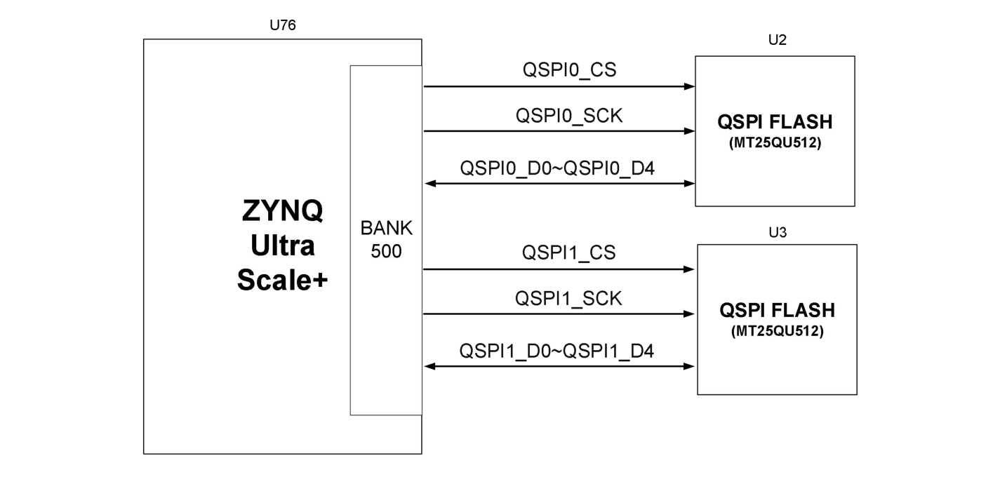
Figure 2.1.3.1 - QSPI Flash Connection Diagram
Configuration chip pin assignment:
| Signal Name | Pin Name | Pin Number |
| MIO5_QSPI0_SS_B | PS_MIO5_500 | AL32 |
| MIO0_QSPI0_SCLK | PS_MIO0_500 | AM33 |
| MIO4_QSPI0_IO0 | PS_MIO4_500 | AL33 |
| MIO1_QSPI0_IO1 | PS_MIO1_500 | AM29 |
| MIO2_QSPI0_IO2 | PS_MIO2_500 | AM31 |
| MIO3_QSPI0_IO3 | PS_MIO3_500 | AM30 |
| MIO7_QSPI1_SS_B | PS_MIO7_500 | AL30 |
| MIO12_QSPI1_SCLK | PS_MIO12_500 | AJ34 |
| MIO8_QSPI1_IO0 | PS_MIO8_500 | AK33 |
| MIO9_QSPI1_IO1 | PS_MIO9_500 | AK34 |
| MIO10_QSPI1_IO2 | PS_MIO10_500 | AK30 |
| MIO11_QSPI1_IO3 | PS_MIO11_500 | AK32 |
Table 2.1.3.2 - QSPI Flash Chip Pin Assignment
2.1.4 eMMC
The ACU19EG SOM is equipped with a large-capacity 32GB eMMC memory chip, model MTFC32GAPALBH-IT. It supports JEDEC e-MMC V5.0 standard HS-MMC interface, with 1.8V or 3.3V voltage level support. The data bus width between the eMMC chip and ZYNQ is 8-bit. Due to its large capacity and non-volatile nature, the eMMC chip can serve as a large-capacity storage device in ZYNQ systems, storing ARM applications, system files, and other user data files. The specific model and parameters of the eMMC memory chip are shown in the table.
| Designator | Chip Type | Capacity | Manufacturer |
| U8 | MTFC32GAPALBH-IT | 32G Byte | Micron |
Table 2.1.4.1 - eMMC Memory Chip Models and Parameters
The eMMC memory chip is connected to the ZYNQ UltraScale+ PS-side BANK 500 GPIO ports. In system design, these PS-side GPIO ports need to be configured as EMMC interface function. The following figure shows the eMMC memory chip section in the schematic.
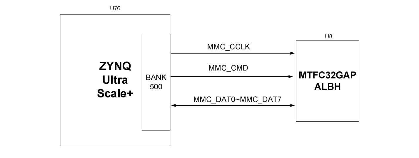
Figure 2.1.4.1 - eMMC Memory Chip Connection Diagram
Configuration chip pin assignment:
| Signal Name | Pin Name | Pin Number |
| MMC_CCLK | PS_MIO22_500 | AH32 |
| MMC_CMD | PS_MIO21_500 | AF35 |
| MMC_DAT0 | PS_MIO13_500 | AD34 |
| MMC_DAT1 | PS_MIO14_500 | AJ32 |
| MMC_DAT2 | PS_MIO15_500 | AD35 |
| MMC_DAT3 | PS_MIO16_500 | AJ31 |
| MMC_DAT4 | PS_MIO17_500 | AJ30 |
| MMC_DAT5 | PS_MIO18_500 | AE34 |
| MMC_DAT6 | PS_MIO19_500 | AE35 |
| MMC_DAT7 | PS_MIO20_500 | AH34 |
| MMC_RSTN | PS_MIO23_500 | AG35 |
Table 2.1.4.2 - eMMC Memory Chip Pin Configuration
2.1.5 Clock Configuration
The SOM provides separate reference clocks and RTC real-time clocks for the PS system and PL logic, allowing them to operate independently. The clock circuit design diagram is shown below.
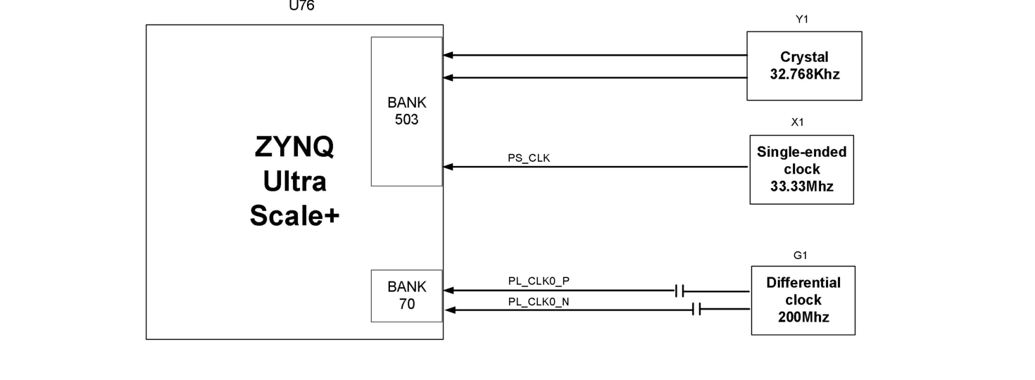
Figure 2.1.5.1 - SOM Clock Sources
PS System RTC Real-Time Clock
The passive crystal Y1 on the SOM provides a 32.768KHz real-time clock source for the PS system. The crystal is connected to the ZYNQ chip BANK 503 pins PS_PADI_503 and PS_PADO_503. The clock pin assignment is shown in the table below.
| Signal Name | Pin |
| PS_PADI_503 | AE28 |
| PS_PADO_503 | AE27 |
Table 2.1.5.1 - PS System RTC Clock Pin Assignment
PS System Clock Source
The X1 oscillator on the SOM provides a 33.333MHz clock input for the PS section. The clock input is connected to the ZYNQ chip BANK 503 pin PS_REF_CLK_503. The clock pin assignment is shown in the table below.
| Signal Name | Pin |
| PS_REF_CLK | AC27 |
Table 2.1.5.2 - PS System Clock Source Pin Assignment
PL System Clock Source
The board provides a differential 200MHz PL system clock source, used as the reference clock for the DDR4 controller. The oscillator output is connected to the PL BANK 71 global clock (MRCC), which can drive the DDR4 controller and user logic circuits within the FPGA. The PL clock pin assignment is shown in the table below.
| Signal Name | Pin |
| PL_CLK0_P | H21 |
| PL_CLK0_N | G20 |
Table 2.1.5.3 - PL System Clock Source Pin Assignment
2.1.6 Power Supply
The ACU19EG SOM is powered by +12V supplied through the carrier board. The SOM uses 1x MAX20796GFB+ power chip delivering 60A to provide the 0.85V core power for the XCZU19EG. Two TPS74801DRCR power chips generate 0.85V and 1.8V for the PS_MGT section. Two MAX20812AFH+ power chips generate two 0.9V and two 1.2V rails for the PL-MGT section. Additionally, a PMIC chip TPS6508640 generates all other power rails required by the XCZU19EG. Refer to the TPS6508640 datasheet for power design details. The design block diagram is shown below:
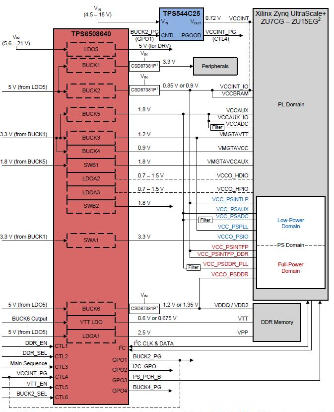
Figure 2.1.6.1 - Power Supply Design Block Diagram
2.1.7 Mechanical Drawing
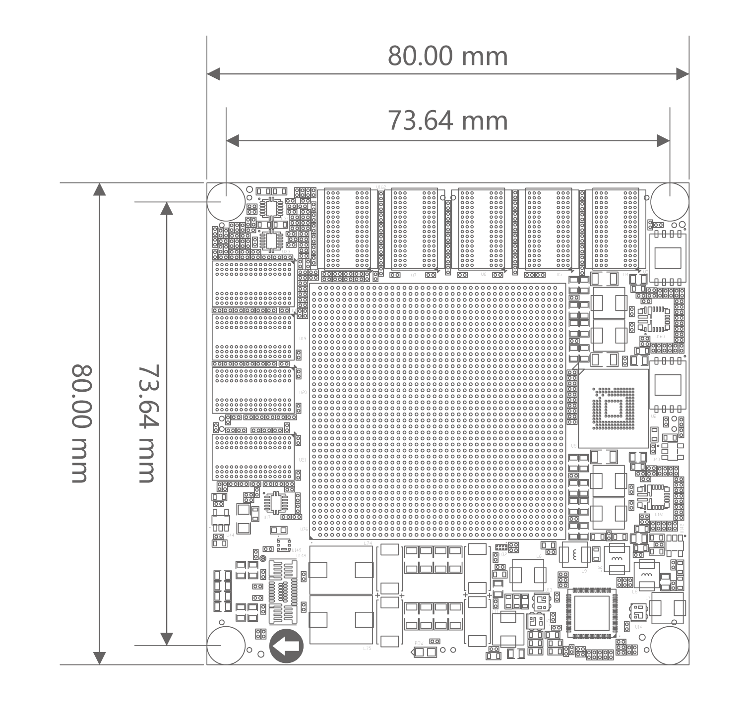
Figure 2.1.7.1 - SOM Top View Mechanical Drawing
2.1.8 Connector Pin Definitions
The SOM expands a total of 8 high-speed expansion ports, using 8x 120-pin board-to-board connectors (J29-J36) to connect to the carrier board. The connectors are Panasonic AXK5A2137YG, and the corresponding carrier board connector model is AXK6A2337YG.
J29 Connector Pin Assignment
J29 connects GTY transceiver signals from BANK 128, 129, 130, 131. The pin assignment table is shown below.
| J29 Pin | Signal Name | Pin Number | J29 Pin | Signal Name | Pin Number |
| 1 | 131_CLK0_P | L32 | 2 | 131_CLK1_P | J32 |
| 3 | 131_CLK0_N | L33 | 4 | 131_CLK1_N | J33 |
| 5 | GND | 6 | GND | ||
| 7 | 131_RX3_P | D39 | 8 | 131_TX3_P | E36 |
| 9 | 131_RX3_N | D40 | 10 | 131_TX3_N | E37 |
| 11 | GND | 12 | GND | ||
| 13 | 131_RX2_P | E41 | 14 | 131_TX2_P | F34 |
| 15 | 131_RX2_N | E42 | 16 | 131_TX2_N | F35 |
| 17 | GND | 18 | GND | ||
| 19 | 131_RX1_P | F39 | 20 | 131_TX1_P | G36 |
| 21 | 131_RX1_N | F40 | 22 | 131_TX1_N | G37 |
| 23 | GND | 24 | GND | ||
| 25 | 131_RX0_P | G41 | 26 | 131_TX0_P | H34 |
| 27 | 131_RX0_N | G42 | 28 | 131_TX0_N | H35 |
| 29 | GND | 30 | GND | ||
| 31 | 130_CLK0_P | R32 | 32 | 130_CLK1_P | N32 |
| 33 | 130_CLK0_N | R33 | 34 | 130_CLK1_N | N33 |
| 35 | GND | 36 | GND | ||
| 37 | 130_RX3_P | H39 | 38 | 130_TX3_P | J36 |
| 39 | 130_RX3_N | H40 | 40 | 130_TX3_N | J37 |
| 41 | GND | 42 | GND | ||
| 43 | 130_RX2_P | J41 | 44 | 130_TX2_P | K34 |
| 45 | 130_RX2_N | J42 | 46 | 130_TX2_N | K35 |
| 47 | GND | 48 | GND | ||
| 49 | 130_RX1_P | K39 | 50 | 130_TX1_P | L36 |
| 51 | 130_RX1_N | K40 | 52 | 130_TX1_N | L37 |
| 53 | GND | 54 | GND | ||
| 55 | 130_RX0_P | L41 | 56 | 130_TX0_P | M34 |
| 57 | 130_RX0_N | L42 | 58 | 130_TX0_N | M35 |
| 59 | GND | 60 | GND | ||
| 61 | 129_CLK0_P | W32 | 62 | 129_CLK1_P | U32 |
| 63 | 129_CLK0_N | W33 | 64 | 129_CLK1_N | U33 |
| 65 | GND | 66 | GND | ||
| 67 | 129_RX3_P | M39 | 68 | 129_TX3_P | N36 |
| 69 | 129_RX3_N | M40 | 70 | 129_TX3_N | N37 |
| 71 | GND | 72 | GND | ||
| 73 | 129_RX2_P | N41 | 74 | 129_TX2_P | P34 |
| 75 | 129_RX2_N | N42 | 76 | 129_TX2_N | P35 |
| 77 | GND | 78 | GND | ||
| 79 | 129_RX1_P | P39 | 80 | 129_TX1_P | R36 |
| 81 | 129_RX1_N | P40 | 82 | 129_TX1_N | R37 |
| 83 | GND | 84 | GND | ||
| 85 | 129_RX0_P | R41 | 86 | 129_TX0_P | T34 |
| 87 | 129_RX0_N | R42 | 88 | 129_TX0_N | T35 |
| 89 | GND | 90 | GND | ||
| 91 | 128_CLK0_P | AB34 | 92 | 128_CLK1_P | AA32 |
| 93 | 128_CLK0_N | AB35 | 94 | 128_CLK1_N | AA33 |
| 95 | GND | 96 | GND | ||
| 97 | 128_RX3_P | T39 | 98 | 128_TX3_P | U36 |
| 99 | 128_RX3_N | T40 | 100 | 128_TX3_N | U37 |
| 101 | GND | 102 | GND | ||
| 103 | 128_RX2_P | U41 | 104 | 128_TX2_P | V34 |
| 105 | 128_RX2_N | U42 | 106 | 128_TX2_N | V35 |
| 107 | GND | 108 | GND | ||
| 109 | 128_RX1_P | V39 | 110 | 128_TX1_P | W36 |
| 111 | 128_RX1_N | V40 | 112 | 128_TX1_N | W37 |
| 113 | GND | 114 | GND | ||
| 115 | 128_RX0_P | W41 | 116 | 128_TX0_P | Y34 |
| 117 | 128_RX0_N | W42 | 118 | 128_TX0_N | Y35 |
| 119 | GND | 120 | GND |
Table 2.1.8.1 - J29 Pin Assignment
J30 Connector
J30 connects BANK 505 MGT transceiver signals, PS MIO, and BANK 28. The PS MIO voltage level is 1.8V standard.
| J30 Pin | Signal Name | Pin Number | J30 Pin | Signal Name | Pin Number |
| 1 | 505_CLK2_N | AC38 | 2 | 505_CLK3_N | AA38 |
| 3 | 505_CLK2_P | AC37 | 4 | 505_CLK3_P | AA37 |
| 5 | GND | 6 | GND | ||
| 7 | 505_TX3_N | AB40 | 8 | 505_RX3_N | AA42 |
| 9 | 505_TX3_P | AB39 | 10 | 505_RX3_P | AA41 |
| 11 | GND | 12 | GND | ||
| 13 | 505_TX2_N | AD40 | 14 | 505_RX2_N | AC42 |
| 15 | 505_TX2_P | AD39 | 16 | 505_RX2_P | AC41 |
| 17 | GND | 18 | GND | ||
| 19 | 505_TX1_N | AF40 | 20 | 505_RX1_N | AE42 |
| 21 | 505_TX1_P | AF39 | 22 | 505_RX1_P | AE41 |
| 23 | GND | 24 | GND | ||
| 25 | 505_TX0_N | AH40 | 26 | 505_RX0_N | AG42 |
| 27 | 505_TX0_P | AH39 | 28 | 505_RX0_P | AG41 |
| 29 | GND | 30 | GND | ||
| 31 | 505_CLK0_N | AG38 | 32 | 505_CLK1_N | AE38 |
| 33 | 505_CLK0_P | AG37 | 34 | 505_CLK1_P | AE37 |
| 35 | GND | 36 | GND | ||
| 37 | DP_HPD_MIO28 | L28 | 38 | DP_AUX_IN_MIO30 | L30 |
| 39 | DP_OE_MIO29 | M27 | 40 | DP_AUX_OUT_MIO27 | L29 |
| 41 | GND | 42 | GND | ||
| 43 | PS_IIC1_SDA | AG34 | 44 | USB_DIR | Y30 |
| 45 | PS_IIC1_SCL | AH33 | 46 | USB_CLK | W29 |
| 47 | SD_CD | T29 | 48 | USB_DATA5 | AC32 |
| 49 | SD_D1 | T28 | 50 | USB_DATA0 | AA30 |
| 51 | GND | 52 | GND | ||
| 53 | SD_D2 | V30 | 54 | USB_DATA3 | AC31 |
| 55 | SD_D3 | U29 | 56 | USB_DATA2 | Y29 |
| 57 | SD_CLK | W30 | 58 | USB_DATA6 | AD31 |
| 59 | SD_CMD | V29 | 60 | USB_DATA1 | AB30 |
| 61 | GND | 62 | GND | ||
| 63 | SD_D0 | U28 | 64 | USB_DATA7 | AD30 |
| 65 | DNC | 66 | USB_NXT | AB29 | |
| 67 | PS_MIO36 | T27 | 68 | USB_STP | AC29 |
| 69 | PCIE_RSTN_MIO37 | N30 | 70 | USB_DATA4 | AD29 |
| 71 | GND | 72 | GND | ||
| 73 | PS_UART_TX | P29 | 74 | PHY1_RXD3 | AG33 |
| 75 | PS_UART_RX | R27 | 76 | PHY1_RXCTL | AF33 |
| 77 | PS_MIO42 | T30 | 78 | PHY1_RXD1 | AF32 |
| 79 | PS_MIO43 | R30 | 80 | PHY1_TXD3 | AE33 |
| 81 | GND | 82 | GND | ||
| 83 | FPGA_DONE | Y28 | 84 | PHY1_RXD0 | AF31 |
| 85 | PS_POR_B | W27 | 86 | PHY1_TXCTL | AE32 |
| 87 | VBAT_IN | 88 | PHY1_RXD2 | AG30 | |
| 89 | PS_MIO44 | R29 | 90 | PHY1_RXCK | AF30 |
| 91 | GND | 92 | GND | ||
| 93 | CAN1_RX | P30 | 94 | PHY1_TXD1 | AD33 |
| 95 | CAN1_TX | P28 | 96 | PHY1_TXD2 | AE30 |
| 97 | CAN0_TX | N29 | 98 | PHY1_TXD0 | AE29 |
| 99 | CAN0_RX | P27 | 100 | PHY1_TXCK | AD32 |
| 101 | GND | 102 | GND | ||
| 103 | PS_UART2_RX | N28 | 104 | PHY1_MDC | AH31 |
| 105 | PS_UART2_TX | M30 | 106 | PHY1_MDIO | AG31 |
| 107 | PS_MIO31 | M28 | 108 | PCIE_PERSTN | AM25 |
| 109 | PS_MIO26 | L27 | 110 | POWER_SW | |
| 111 | GND | 112 | GND | ||
| 113 | PS_MODE2 | AA28 | 114 | PS_MODE3 | AB28 |
| 115 | PS_MODE0 | AA27 | 116 | PS_MODE1 | AC28 |
| 117 | FPGA_TDO | AD27 | 118 | FPGA_TMS | AD26 |
| 119 | FPGA_TCK | AC26 | 120 | FPGA_TDI | AD25 |
Table 2.1.8.2 - J30 Pin Assignment
J31 Connector
J31 connects BANK 64 and BANK 65 IO. The maximum voltage level for BANK 64, 65 is +1.8V.
| J31 Pin | Signal Name | Pin Number | J31 Pin | Signal Name | Pin Number |
| 1 | B65_L10_N | AV28 | 2 | B65_L18_N | AT28 |
| 3 | B65_L10_P | AU28 | 4 | B65_L18_P | AR28 |
| 5 | B65_L16_N | AP27 | 6 | B65_L15_N | AN26 |
| 7 | B65_L16_P | AN27 | 8 | B65_L15_P | AM26 |
| 9 | GND | 10 | GND | ||
| 11 | B65_L13_N | AT27 | 12 | B65_L9_N | AW27 |
| 13 | B65_L13_P | AR27 | 14 | B65_L9_P | AV27 |
| 15 | B65_L5_N | AY28 | 16 | B65_L12_N | AT26 |
| 17 | B65_L5_P | AY27 | 18 | B65_L12_P | AT25 |
| 19 | GND | 20 | GND | ||
| 21 | B65_L8_N | AW26 | 22 | B65_L11_N | AU26 |
| 23 | B65_L8_P | AV26 | 24 | B65_L11_P | AU25 |
| 25 | B65_L20_N | AP25 | 26 | B65_L6_N | BB28 |
| 27 | B65_L20_P | AP24 | 28 | B65_L6_P | BA28 |
| 29 | GND | 30 | GND | ||
| 31 | B65_L4_N | BB26 | 32 | B65_L14_N | AR25 |
| 33 | B65_L4_P | BA26 | 34 | B65_L14_P | AR24 |
| 35 | B65_L2_N | BB25 | 36 | B65_L3_N | BA25 |
| 37 | B65_L2_P | BB24 | 38 | B65_L3_P | AY25 |
| 39 | GND | 40 | GND | ||
| 41 | B65_L7_N | AV24 | 42 | B65_L1_N | AY24 |
| 43 | B65_L7_P | AU24 | 44 | B65_L1_P | AW24 |
| 45 | B65_L21_N | AN24 | 46 | B65_L22_N | AN23 |
| 47 | B65_L21_P | AM24 | 48 | B65_L22_P | AM23 |
| 49 | GND | 50 | GND | ||
| 51 | B65_L19_N | AT23 | 52 | B65_L23_N | AL23 |
| 53 | B65_L19_P | AR23 | 54 | B65_L23_P | AK23 |
| 55 | B65_L24_N | AK24 | 56 | B65_L17_N | AN28 |
| 57 | B65_L24_P | AJ24 | 58 | B65_L17_P | AM28 |
| 59 | GND | 60 | GND | ||
| 61 | B64_L23_P | AJ21 | 62 | B64_L1_P | BA23 |
| 63 | B64_L23_N | AJ20 | 64 | B64_L1_N | BB23 |
| 65 | B64_L24_P | AJ22 | 66 | B64_L16_P | AN21 |
| 67 | B64_L24_N | AK22 | 68 | B64_L16_N | AP21 |
| 69 | GND | 70 | GND | ||
| 71 | B64_L7_P | AU23 | 72 | B64_L22_P | AK20 |
| 73 | B64_L7_N | AV23 | 74 | B64_L22_N | AK19 |
| 75 | B64_L2_P | AY23 | 76 | B64_L19_P | AM19 |
| 77 | B64_L2_N | AY22 | 78 | B64_L19_N | AN19 |
| 79 | GND | 80 | GND | ||
| 81 | B64_L20_P | AM21 | 82 | B64_L14_P | AT20 |
| 83 | B64_L20_N | AM20 | 84 | B64_L14_N | AU19 |
| 85 | B64_L11_P | AU21 | 86 | B64_L3_P | BA22 |
| 87 | B64_L11_N | AV21 | 88 | B64_L3_N | BA21 |
| 89 | GND | 90 | GND | ||
| 91 | B64_L18_P | AP19 | 92 | B64_L5_P | BB20 |
| 93 | B64_L18_N | AR19 | 94 | B64_L5_N | BB19 |
| 95 | B64_L8_P | AV22 | 96 | B64_L6_P | BA18 |
| 97 | B64_L8_N | AW22 | 98 | B64_L6_N | BB18 |
| 99 | GND | 100 | GND | ||
| 101 | B64_L21_P | AL22 | 102 | B64_L9_P | AW20 |
| 103 | B64_L21_N | AL21 | 104 | B64_L9_N | AW19 |
| 105 | B64_L15_P | AN22 | 106 | B64_L10_P | AY19 |
| 107 | B64_L15_N | AP22 | 108 | B64_L10_N | AY18 |
| 109 | GND | 110 | GND | ||
| 111 | B64_L13_P | AT22 | 112 | B64_L4_P | AY20 |
| 113 | B64_L13_N | AT21 | 114 | B64_L4_N | BA20 |
| 115 | B64_L17_P | AP20 | 116 | B64_L12_P | AU20 |
| 117 | B64_L17_N | AR20 | 118 | B64_L12_N | AV19 |
| 119 | GND | 120 | GND |
Table 2.1.8.3 - J31 Pin Assignment
J32 Connector
J32 connects BANK 66 and BANK 67 IO. The maximum voltage level for BANK 66, 67 is +1.8V.
| J32 Pin | Signal Name | Pin Number | J32 Pin | Signal Name | Pin Number |
| 1 | B66_L3_P | AW17 | 2 | B66_L4_P | BA15 |
| 3 | B66_L3_N | AW16 | 4 | B66_L4_N | BB15 |
| 5 | B66_L1_P | AY17 | 6 | B66_L15_P | AU18 |
| 7 | B66_L1_N | BA17 | 8 | B66_L15_N | AV18 |
| 9 | GND | 10 | GND | ||
| 11 | B66_L13_P | AV17 | 12 | B66_L16_P | AR18 |
| 13 | B66_L13_N | AV16 | 14 | B66_L16_N | AT18 |
| 15 | B66_L17_P | AR17 | 16 | B66_L2_P | BA16 |
| 17 | B66_L17_N | AT17 | 18 | B66_L2_N | BB16 |
| 19 | GND | 20 | GND | ||
| 21 | B66_L5_P | AY15 | 22 | B66_L20_P | AL18 |
| 23 | B66_L5_N | AY14 | 24 | B66_L20_N | AM18 |
| 25 | B66_L19_P | AJ18 | 26 | B66_L21_P | AN18 |
| 27 | B66_L19_N | AK18 | 28 | B66_L21_N | AN17 |
| 29 | GND | 30 | GND | ||
| 31 | B66_L11_P | AW15 | 32 | B66_L14_P | AT15 |
| 33 | B66_L11_N | AW14 | 34 | B66_L14_N | AU15 |
| 35 | B66_L24_P | AN16 | 36 | B66_L18_P | AT16 |
| 37 | B66_L24_N | AP16 | 38 | B66_L18_N | AU16 |
| 39 | GND | 40 | GND | ||
| 41 | B66_L22_P | AJ17 | 42 | B66_L23_P | AL16 |
| 43 | B66_L22_N | AK17 | 44 | B66_L23_N | AM16 |
| 45 | B66_L10_P | AU13 | 46 | B66_L12_P | AU14 |
| 47 | B66_L10_N | AV13 | 48 | B66_L12_N | AV14 |
| 49 | GND | 50 | GND | ||
| 51 | B66_L7_P | AY12 | 52 | B66_L9_P | BA10 |
| 53 | B66_L7_N | BA12 | 54 | B66_L9_N | BB10 |
| 55 | B66_L8_P | BA11 | 56 | B66_L6_P | BA13 |
| 57 | B66_L8_N | BB11 | 58 | B66_L6_N | BB13 |
| 59 | GND | 60 | GND | ||
| 61 | B67_L23_P | AM13 | 62 | B67_L15_P | AR15 |
| 63 | B67_L23_N | AN13 | 64 | B67_L15_N | AR14 |
| 65 | B67_L12_P | AT11 | 66 | B67_L7_P | AV12 |
| 67 | B67_L12_N | AT10 | 68 | B67_L7_N | AW12 |
| 69 | GND | 70 | GND | ||
| 71 | B67_L16_P | AN12 | 72 | B67_L11_P | AT13 |
| 73 | B67_L16_N | AP12 | 74 | B67_L11_N | AT12 |
| 75 | B67_L14_P | AP10 | 76 | B67_L13_P | AR13 |
| 77 | B67_L14_N | AR10 | 78 | B67_L13_N | AR12 |
| 79 | GND | 80 | GND | ||
| 81 | B67_L9_P | AW11 | 82 | B67_L24_P | AJ14 |
| 83 | B67_L9_N | AW10 | 84 | B67_L24_N | AK14 |
| 85 | B67_L3_P | AW8 | 86 | B67_L22_P | AN14 |
| 87 | B67_L3_N | AY8 | 88 | B67_L22_N | AP14 |
| 89 | GND | 90 | GND | ||
| 91 | B67_L1_P | AW9 | 92 | B67_L19_P | AL15 |
| 93 | B67_L1_N | AY9 | 94 | B67_L19_N | AM15 |
| 95 | B67_L20_P | AJ15 | 96 | B67_L17_P | AM11 |
| 97 | B67_L20_N | AK15 | 98 | B67_L17_N | AN11 |
| 99 | GND | 100 | GND | ||
| 101 | B67_L4_P | BA8 | 102 | B67_L21_P | AL14 |
| 103 | B67_L4_N | BA7 | 104 | B67_L21_N | AM14 |
| 105 | B67_L10_P | AV9 | 106 | B67_L8_P | AU11 |
| 107 | B67_L10_N | AV8 | 108 | B67_L8_N | AV11 |
| 109 | GND | 110 | GND | ||
| 111 | B67_L2_P | BB9 | 112 | B67_L5_P | BA6 |
| 113 | B67_L2_N | BB8 | 114 | B67_L5_N | BB6 |
| 115 | B67_L6_P | BB5 | 116 | B67_L18_P | AM10 |
| 117 | B67_L6_N | BB4 | 118 | B67_L18_N | AN10 |
| 119 | GND | 120 | GND |
Table 2.1.8.4 - J32 Pin Assignment
J33 Connector Pin Assignment
J33 connects GTH transceiver signals from BANK 224, 225, 226, 227.
| J33 Pin | Signal Name | Pin Number | J33 Pin | Signal Name | Pin Number |
| 1 | 224_TX0_N | AY3 | 2 | 224_RX0_N | BA1 |
| 3 | 224_TX0_P | AY4 | 4 | 224_RX0_P | BA2 |
| 5 | GND | 6 | GND | ||
| 7 | 224_TX1_N | AW5 | 8 | 224_RX1_N | AW1 |
| 9 | 224_TX1_P | AW6 | 10 | 224_RX1_P | AW2 |
| 11 | GND | 12 | GND | ||
| 13 | 224_TX2_N | AU5 | 14 | 224_RX2_N | AV3 |
| 15 | 224_TX2_P | AU6 | 16 | 224_RX2_P | AV4 |
| 17 | GND | 18 | GND | ||
| 19 | 224_TX3_N | AT7 | 20 | 224_RX3_N | AU1 |
| 21 | 224_TX3_P | AT8 | 22 | 224_RX3_P | AU2 |
| 23 | GND | 24 | GND | ||
| 25 | 224_CLK0_N | AK11 | 26 | 224_CLK1_N | AJ9 |
| 27 | 224_CLK0_P | AK12 | 28 | 224_CLK1_P | AJ10 |
| 29 | GND | 30 | GND | ||
| 31 | 225_TX0_N | AR5 | 32 | 225_RX0_N | AT3 |
| 33 | 225_TX0_P | AR6 | 34 | 225_RX0_P | AT4 |
| 35 | GND | 36 | GND | ||
| 37 | 225_TX1_N | AP7 | 38 | 225_RX1_N | AR1 |
| 39 | 225_TX1_P | AP8 | 40 | 225_RX1_P | AR2 |
| 41 | GND | 42 | GND | ||
| 43 | 225_TX2_N | AN5 | 44 | 225_RX2_N | AP3 |
| 45 | 225_TX2_P | AN6 | 46 | 225_RX2_P | AP4 |
| 47 | GND | 48 | GND | ||
| 49 | 225_TX3_N | AM7 | 50 | 225_RX3_N | AN1 |
| 51 | 225_TX3_P | AM8 | 52 | 225_RX3_P | AN2 |
| 53 | GND | 54 | GND | ||
| 55 | 225_CLK0_N | AH11 | 56 | 225_CLK1_N | AG9 |
| 57 | 225_CLK0_P | AH12 | 58 | 225_CLK1_P | AG10 |
| 59 | GND | 60 | GND | ||
| 61 | 226_TX0_N | AL5 | 62 | 226_RX0_N | AM3 |
| 63 | 226_TX0_P | AL6 | 64 | 226_RX0_P | AM4 |
| 65 | GND | 66 | GND | ||
| 67 | 226_TX1_N | AK7 | 68 | 226_RX1_N | AL1 |
| 69 | 226_TX1_P | AK8 | 70 | 226_RX1_P | AL2 |
| 71 | GND | 72 | GND | ||
| 73 | 226_TX2_N | AJ5 | 74 | 226_RX2_N | AK3 |
| 75 | 226_TX2_P | AJ6 | 76 | 226_RX2_P | AK4 |
| 77 | GND | 78 | GND | ||
| 79 | 226_TX3_N | AH7 | 80 | 226_RX3_N | AJ1 |
| 81 | 226_TX3_P | AH8 | 82 | 226_RX3_P | AJ2 |
| 83 | GND | 84 | GND | ||
| 85 | 226_CLK0_N | AF11 | 86 | 226_CLK1_N | AE9 |
| 87 | 226_CLK0_P | AF12 | 88 | 226_CLK1_P | AE10 |
| 89 | GND | 90 | GND | ||
| 91 | 227_TX0_N | AG5 | 92 | 227_RX0_N | AH3 |
| 93 | 227_TX0_P | AG6 | 94 | 227_RX0_P | AH4 |
| 95 | GND | 96 | GND | ||
| 97 | 227_TX1_N | AF7 | 98 | 227_RX1_N | AG1 |
| 99 | 227_TX1_P | AF8 | 100 | 227_RX1_P | AG2 |
| 101 | GND | 102 | GND | ||
| 103 | 227_TX2_N | AE5 | 104 | 227_RX2_N | AF3 |
| 105 | 227_TX2_P | AE6 | 106 | 227_RX2_P | AF4 |
| 107 | GND | 108 | GND | ||
| 109 | 227_TX3_N | AD7 | 110 | 227_RX3_N | AE1 |
| 111 | 227_TX3_P | AD8 | 112 | 227_RX3_P | AE2 |
| 113 | GND | 114 | GND | ||
| 115 | 227_CLK0_N | AD11 | 116 | 227_CLK1_N | AC9 |
| 117 | 227_CLK0_P | AD12 | 118 | 227_CLK1_P | AC10 |
| 119 | GND | 120 | GND |
Table 2.1.8.5 - J33 Pin Assignment
J34 Connector Pin Assignment
J34 connects GTH transceiver signals from BANK 228, 229, 230, 231.
| J34 Pin | Signal Name | Pin Number | J34 Pin | Signal Name | Pin Number |
| 1 | 228_TX0_N | AC5 | 2 | 228_RX0_N | AD3 |
| 3 | 228_TX0_P | AC6 | 4 | 228_RX0_P | AD4 |
| 5 | GND | 6 | GND | ||
| 7 | 228_TX1_N | AB7 | 8 | 228_RX1_N | AC1 |
| 9 | 228_TX1_P | AB8 | 10 | 228_RX1_P | AC2 |
| 11 | GND | 12 | GND | ||
| 13 | 228_TX2_N | AA5 | 14 | 228_RX2_N | AB3 |
| 15 | 228_TX2_P | AA6 | 16 | 228_RX2_P | AB4 |
| 17 | GND | 18 | GND | ||
| 19 | 228_TX3_N | Y7 | 20 | 228_RX3_N | AA1 |
| 21 | 228_TX3_P | Y8 | 22 | 228_RX3_P | AA2 |
| 23 | GND | 24 | GND | ||
| 25 | 228_CLK1_N | AA9 | 26 | 228_CLK0_N | AB11 |
| 27 | 228_CLK1_P | AA10 | 28 | 228_CLK0_P | AB12 |
| 29 | GND | 30 | GND | ||
| 31 | 229_TX0_N | W5 | 32 | 229_RX0_N | Y3 |
| 33 | 229_TX0_P | W6 | 34 | 229_RX0_P | Y4 |
| 35 | GND | 36 | GND | ||
| 37 | 229_TX1_N | V7 | 38 | 229_RX1_N | W1 |
| 39 | 229_TX1_P | V8 | 40 | 229_RX1_P | W2 |
| 41 | GND | 42 | GND | ||
| 43 | 229_TX2_N | U5 | 44 | 229_RX2_N | V3 |
| 45 | 229_TX2_P | U6 | 46 | 229_RX2_P | V4 |
| 47 | GND | 48 | GND | ||
| 49 | 229_TX3_N | T7 | 50 | 229_RX3_N | U1 |
| 51 | 229_TX3_P | T8 | 52 | 229_RX3_P | U2 |
| 53 | GND | 54 | GND | ||
| 55 | 229_CLK1_N | W9 | 56 | 229_CLK0_N | Y11 |
| 57 | 229_CLK1_P | W10 | 58 | 229_CLK0_P | Y12 |
| 59 | GND | 60 | GND | ||
| 61 | 230_TX0_N | R5 | 62 | 230_RX0_N | T3 |
| 63 | 230_TX0_P | R6 | 64 | 230_RX0_P | T4 |
| 65 | GND | 66 | GND | ||
| 67 | 230_TX1_N | P7 | 68 | 230_RX1_N | R1 |
| 69 | 230_TX1_P | P8 | 70 | 230_RX1_P | R2 |
| 71 | GND | 72 | GND | ||
| 73 | 230_TX2_N | N5 | 74 | 230_RX2_N | P3 |
| 75 | 230_TX2_P | N6 | 76 | 230_RX2_P | P4 |
| 77 | GND | 78 | GND | ||
| 79 | 230_TX3_N | M7 | 80 | 230_RX3_N | N1 |
| 81 | 230_TX3_P | M8 | 82 | 230_RX3_P | N2 |
| 83 | GND | 84 | GND | ||
| 85 | 230_CLK1_N | U9 | 86 | 230_CLK0_N | V11 |
| 87 | 230_CLK1_P | U10 | 88 | 230_CLK0_P | V12 |
| 89 | GND | 90 | GND | ||
| 91 | 231_TX0_N | L5 | 92 | 231_RX0_N | M3 |
| 93 | 231_TX0_P | L6 | 94 | 231_RX0_P | M4 |
| 95 | GND | 96 | GND | ||
| 97 | 231_TX1_N | K3 | 98 | 231_RX1_N | L1 |
| 99 | 231_TX1_P | K4 | 100 | 231_RX1_P | L2 |
| 101 | GND | 102 | GND | ||
| 103 | 231_TX2_N | J5 | 104 | 231_RX2_N | J1 |
| 105 | 231_TX2_P | J6 | 106 | 231_RX2_P | J2 |
| 107 | GND | 108 | GND | AC20 | |
| 109 | 231_TX3_N | H3 | 110 | 231_RX3_N | G1 |
| 111 | 231_TX3_P | H4 | 112 | 231_RX3_P | G2 |
| 113 | GND | 114 | GND | ||
| 115 | 231_CLK1_N | R9 | 116 | 231_CLK0_N | T11 |
| 117 | 231_CLK1_P | R10 | 118 | 231_CLK0_P | T12 |
| 119 | GND | 120 | GND |
Table 2.1.8.6 - J34 Pin Assignment
J35 Connector
J35 connects +12V power, and BANK 91, BANK 93, BANK 94 IO. The voltage level for BANK 91, 93, 94 is 3.3V.
| J35 Pin | Signal Name | Pin Number | J35 Pin | Signal Name | Pin Number |
| 1 | +12V | 2 | GND | ||
| 3 | +12V | 4 | GND | ||
| 5 | +12V | 6 | GND | ||
| 7 | +12V | 8 | GND | ||
| 9 | +12V | 10 | GND | ||
| 11 | +12V | 12 | GND | ||
| 13 | +12V | 14 | GND | ||
| 15 | +12V | 16 | GND | ||
| 17 | +12V | 18 | GND | ||
| 19 | +12V | 20 | GND | ||
| 21 | +12V | 22 | GND | ||
| 23 | +12V | 24 | GND | ||
| 25 | +12V | 26 | GND | ||
| 27 | +12V | 28 | GND | ||
| 29 | +12V | 30 | GND | ||
| 31 | GND | 32 | GND | ||
| 33 | B94_L5_N | D3 | 34 | B94_L8_N | C3 |
| 35 | B94_L5_P | D4 | 36 | B94_L8_P | C4 |
| 37 | B94_L7_N | C5 | 38 | B94_L12_N | A4 |
| 39 | B94_L7_P | C6 | 40 | B94_L12_P | A5 |
| 41 | GND | 42 | GND | ||
| 43 | B94_L3_N | E2 | 44 | B94_L4_N | D1 |
| 45 | B94_L3_P | E3 | 46 | B94_L4_P | E1 |
| 47 | B94_L6_N | C1 | 48 | B94_L9_N | B1 |
| 49 | B94_L6_P | D2 | 50 | B94_L9_P | B2 |
| 51 | GND | 52 | GND | ||
| 53 | B94_L1_N | F4 | 54 | B94_L11_N | B5 |
| 55 | B94_L1_P | F5 | 56 | B94_L11_P | B6 |
| 57 | B94_L10_N | A3 | 58 | B94_L2_N | E4 |
| 59 | B94_L10_P | B3 | 60 | B94_L2_P | E5 |
| 61 | GND | 62 | GND | ||
| 63 | B93_L10_N | A7 | 64 | B93_L1_N | F6 |
| 65 | B93_L10_P | B7 | 66 | B93_L1_P | G6 |
| 67 | B93_L9_N | D6 | 68 | B93_L5_N | F7 |
| 69 | B93_L9_P | E6 | 70 | B93_L5_P | G7 |
| 71 | GND | 72 | GND | ||
| 73 | B93_L7_N | D7 | 74 | B93_L2_N | H8 |
| 75 | B93_L7_P | E7 | 76 | B93_L2_P | J8 |
| 77 | B93_L8_N | C8 | 78 | B93_L4_N | E9 |
| 79 | B93_L8_P | D8 | 80 | B93_L4_P | F9 |
| 81 | GND | 82 | GND | ||
| 83 | B93_L3_N | H9 | 84 | B93_L6_N | F8 |
| 85 | B93_L3_P | J9 | 86 | B93_L6_P | G8 |
| 87 | B93_L11_N | A8 | 88 | B93_L12_N | C9 |
| 89 | B93_L11_P | B8 | 90 | B93_L12_P | D9 |
| 91 | GND | 92 | GND | ||
| 93 | B91_L12_N | A9 | 94 | B91_L7_N | E10 |
| 95 | B91_L12_P | A10 | 96 | B91_L7_P | E11 |
| 97 | B91_L5_N | F10 | 98 | B91_L1_N | H10 |
| 99 | B91_L5_P | G10 | 100 | B91_L1_P | J11 |
| 101 | GND | 102 | GND | ||
| 103 | B91_L10_N | B10 | 104 | B91_L9_N | C11 |
| 105 | B91_L10_P | C10 | 106 | B91_L9_P | D11 |
| 107 | B91_L11_N | B11 | 108 | B91_L2_N | G11 |
| 109 | B91_L11_P | B12 | 110 | B91_L2_P | H11 |
| 111 | GND | 112 | GND | ||
| 113 | B91_L3_N | G12 | 114 | B91_L8_N | D12 |
| 115 | B91_L3_P | H13 | 116 | B91_L8_P | E12 |
| 117 | B91_L4_N | G13 | 118 | B91_L6_N | F12 |
| 119 | B91_L4_P | H14 | 120 | B91_L6_P | F13 |
Table 2.1.8.7 - J35 Pin Assignment
J36 Connector
J36 connects VCCIO 64-68 BANK power, and BANK 68, BANK 90 IO. BANK 68 voltage level is +1.8V, BANK 90 voltage level is +3.3V.
| J36 Pin | Signal Name | Pin Number | J36 Pin | Signal Name | Pin Number |
| 1 | VCCO_68 | 2 | B68_L16_N | A12 | |
| 3 | VCCO_68 | 4 | B68_L16_P | B13 | |
| 5 | GND | 6 | B68_L17_N | A13 | |
| 7 | GND | 8 | B68_L17_P | A14 | |
| 9 | VCCO_67 | 10 | GND | ||
| 11 | VCCO_67 | 12 | B68_L15_N | C13 | |
| 13 | GND | 14 | B68_L15_P | D13 | |
| 15 | GND | 16 | B68_L1_N | N15 | |
| 17 | VCCO_66 | 18 | B68_L1_P | P15 | |
| 19 | VCCO_66 | 20 | GND | ||
| 21 | GND | 22 | B68_L14_N | D14 | |
| 23 | GND | 24 | B68_L14_P | E15 | |
| 25 | VCCO_64 | 26 | B68_L13_N | E14 | |
| 27 | VCCO_64 | 28 | B68_L13_P | F14 | |
| 29 | GND | 30 | GND | ||
| 31 | GND | 32 | B68_L18_N | B15 | |
| 33 | VCCO_65 | 34 | B68_L18_P | C15 | |
| 35 | VCCO_65 | 36 | B68_L12_N | F15 | |
| 37 | GND | 38 | B68_L12_P | G16 | |
| 39 | GND | 40 | GND | ||
| 41 | DNC | 42 | B68_L20_N | B16 | |
| 43 | DNC | 44 | B68_L20_P | C16 | |
| 45 | DNC | 46 | B68_L19_N | D16 | |
| 47 | DNC | 48 | B68_L19_P | E16 | |
| 49 | GND | 50 | GND | ||
| 51 | DNC | 52 | B68_L22_N | A17 | |
| 53 | DNC | 54 | B68_L22_P | B17 | |
| 55 | DNC | 56 | B68_L21_N | D17 | |
| 57 | DNC | 58 | B68_L21_P | E17 | |
| 59 | GND | 60 | GND | ||
| 61 | B90_L12_N | J12 | 62 | B68_L24_N | A18 |
| 63 | B90_L12_P | J13 | 64 | B68_L24_P | B18 |
| 65 | B90_L7_N | K12 | 66 | B68_L23_N | C18 |
| 67 | B90_L7_P | L12 | 68 | B68_L23_P | D18 |
| 69 | GND | 70 | GND | ||
| 71 | B90_L10_N | K10 | 72 | B68_L7_N | G15 |
| 73 | B90_L10_P | K11 | 74 | B68_L7_P | H15 |
| 75 | B90_L8_N | L13 | 76 | B68_L5_N | K15 |
| 77 | B90_L8_P | L14 | 78 | B68_L5_P | K16 |
| 79 | GND | 80 | GND | ||
| 81 | B90_L11_N | J14 | 82 | B68_L11_N | F17 |
| 83 | B90_L11_P | K14 | 84 | B68_L11_P | G17 |
| 85 | B90_L5_N | M13 | 86 | B68_L10_N | F18 |
| 87 | B90_L5_P | N13 | 88 | B68_L10_P | G18 |
| 89 | GND | 90 | GND | ||
| 91 | B90_L4_N | N14 | 92 | B68_L8_N | H16 |
| 93 | B90_L4_P | P14 | 94 | B68_L8_P | J16 |
| 95 | B90_L3_N | P13 | 96 | B68_L6_N | K17 |
| 97 | B90_L3_P | R14 | 98 | B68_L6_P | L17 |
| 99 | GND | 100 | GND | ||
| 101 | B90_L2_N | N12 | 102 | B68_L9_N | H18 |
| 103 | B90_L2_P | P12 | 104 | B68_L9_P | J18 |
| 105 | B90_L9_N | L10 | 106 | B68_L3_N | M16 |
| 107 | B90_L9_P | M10 | 108 | B68_L3_P | M17 |
| 109 | GND | 110 | GND | ||
| 111 | B90_L6_N | M11 | 112 | B68_L4_N | L15 |
| 113 | B90_L6_P | M12 | 114 | B68_L4_P | M15 |
| 115 | B90_L1_N | N10 | 116 | B68_L2_N | N16 |
| 117 | B90_L1_P | N11 | 118 | B68_L2_P | P16 |
| 119 | GND | 120 | GND |
Table 2.1.8.8 - J36 Pin Assignment
2.2 M.2 Interface
The carrier board MPSoC system is equipped with a PCIe x1 standard M.2 interface for connecting M.2 SSD solid-state drives, with a data transfer rate up to 5Gbps. The M.2 interface uses an M-key slot, supporting only PCIe (not SATA). Users should select PCIe-type SSD solid-state drives when choosing an SSD.
The PCIe signals are directly connected to the ZU19EG BANK 505 PS MGT transceiver. One TX and one RX signal pair are connected differentially to MGT LANE1. The PCIe clock is provided by the Si5332 chip at a frequency of 100MHz. The M.2 circuit design diagram is shown below:
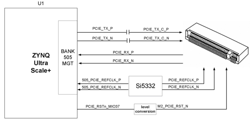
Figure 2.2.1 - M.2 Interface Design Diagram
M.2 interface ZYNQ pin assignment is as follows:
| Signal Name | Pin Name | Pin Number | Remarks |
| PCIE_TX_P | PS_MGTRTXP0_505 | AH39 | PCIe data transmit positive |
| PCIE_TX_N | PS_MGTRTXN0_505 | AH40 | PCIe data transmit negative |
| PCIE_RX_P | PS_MGTRRXP0_505 | AG41 | PCIe data receive positive |
| PCIE_RX_N | PS_MGTRRXN0_505 | AG42 | PCIe data receive negative |
| 505_PCIE_REFCLK_P | PS_MGTREFCLK0P_505 | AG37 | PCIe reference clock positive |
| 505_PCIE_REFCLK_N | PS_MGTREFCLK0N_505 | AG38 | PCIe reference clock negative |
| PCIE_RSTN_MIO37 | PS_MIO37_501 | N30 | PCIe reset signal |
Table 2.2.1 - M.2 Pin Configuration
2.3 DP Display Interface
The carrier board MPSoC system has 1x mini DisplayPort output interface for video display. The interface supports VESA DisplayPort V1.2a output standard, up to 4K x 2K@30fps output, and supports Y-only, YCbCr444, YCbCr422, YCbCr420, and RGB video formats, with 6, 8, 10, or 12 bits per color.
The DisplayPort data transmission channels are directly driven by the ZU19EG BANK 505 PS MGT. The MGT LANE2 and LANE3 TX signals are connected differentially to the DP connector. The DisplayPort auxiliary channel is connected to the PS MIO pins. The DP output interface design diagram is shown below:
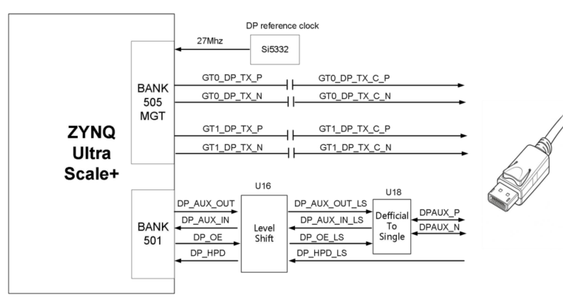
Figure 2.3.1 - DP Interface Design Diagram
DisplayPort interface ZYNQ pin assignment is as follows:
| Signal Name | ZYNQ Pin Name | ZYNQ Pin Number | Remarks |
| GT0_DP_TX_P | PS_MGTRTXP3_505 | AB39 | DP data low lane transmit positive |
| GT0_DP_TX_N | PS_MGTRTXN3_505 | AB40 | DP data low lane transmit negative |
| GT1_DP_TX_P | PS_MGTRTXP2_505 | AD39 | DP data high lane transmit positive |
| GT1_DP_TX_N | PS_MGTRTXN2_505 | AD40 | DP data high lane transmit negative |
| 505_DP_CLKP | PS_MGTREFCLK2P_505 | AC37 | DP reference clock positive |
| 505_DP_CLKN | PS_MGTREFCLK2N_505 | AC38 | DP reference clock negative |
| DP_AUX_OUT_MIO27 | PS_MIO27_501 | L29 | DP auxiliary data output |
| DP_AUX_IN_MIO30 | PS_MIO30_501 | L30 | DP auxiliary data input |
| DP_OE_MIO29 | PS_MIO29_501 | M27 | DP auxiliary data output enable |
| DP_HPD_MIO28 | PS_MIO28_501 | L28 | DP hot plug detect |
Table 2.3.1 - DisplayPort Pin Assignment
2.4 USB3.0 Type-C Interface
The carrier board MPSoC system has 1x USB3.0 Type-C interface, supporting HOST, SLAVE, and OTG modes, with a data transfer rate up to 5.0Gb/s. USB3.0 is connected via the PIPE3 interface, and USB2.0 is connected via the ULPI interface to the external USB3320C chip, enabling high-speed USB3.0 and USB2.0 data communication. The USB3.0 connection diagram is shown below:
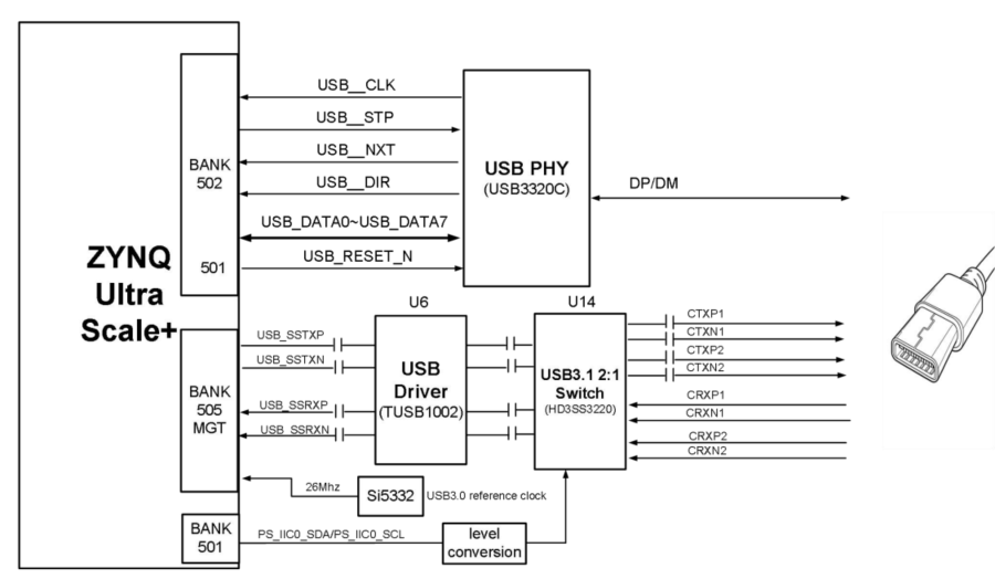
Figure 2.4.1 - USB3.0 Interface Diagram
The USB interface pin assignment is shown in the table below.
| Signal Name | Pin Name | Pin Number | Remarks |
| USB_SSTXP | PS_MGTRTXP1_505 | AF39 | USB3.0 data transmit positive |
| USB_SSTXN | PS_MGTRTXN1_505 | AF40 | USB3.0 data transmit negative |
| USB_SSRXP | PS_MGTRRXP1_505 | AE41 | USB3.0 data receive positive |
| USB_SSRXN | PS_MGTRRXN1_505 | AE42 | USB3.0 data receive negative |
| USB_DATA0 | PS_MIO56_502 | AA30 | USB2.0 data Bit0 |
| USB_DATA1 | PS_MIO57_502 | AB30 | USB2.0 data Bit1 |
| USB_DATA2 | PS_MIO54_502 | Y29 | USB2.0 data Bit2 |
| USB_DATA3 | PS_MIO59_502 | AC31 | USB2.0 data Bit3 |
| USB_DATA4 | PS_MIO60_502 | AD29 | USB2.0 data Bit4 |
| USB_DATA5 | PS_MIO61_502 | AC32 | USB2.0 data Bit5 |
| USB_DATA6 | PS_MIO62_502 | AD31 | USB2.0 data Bit6 |
| USB_DATA7 | PS_MIO63_502 | AD30 | USB2.0 data Bit7 |
| USB_STP | PS_MIO58_502 | AC29 | USB2.0 stop signal |
| USB_DIR | PS_MIO53_502 | Y30 | USB2.0 data direction signal |
| USB_CLK | PS_MIO52_502 | W29 | USB2.0 clock signal |
| USB_NXT | PS_MIO55_502 | AB29 | USB2.0 next data signal |
| USB_RESET_N | PS_MIO44_501 | R29 | USB2.0 reset signal |
Table 2.4.1 - USB Pin Assignment
2.5 Gigabit Ethernet Interface
The carrier board has 1x Gigabit Ethernet interface connected to the PS side. The Ethernet chip uses MicroChip's industrial-grade GPHY chip (KSZ9031RNX) to provide network communication services. The PS-side Ethernet PHY chip is connected to the ZYNQ PS-side BANK 502 GPIO interface. The KSZ9031RNX chip supports 10/100/1000 Mbps network data rates, communicating with the ZYNQ system MAC layer via the RGMII interface. The KSZ9031RNX supports MDI/MDX auto-negotiation, speed auto-negotiation, Master/Slave auto-negotiation, and MDIO bus for PHY register management.
The KSZ9031RNX detects the voltage levels of specific IO pins upon power-up to determine its operating mode. The table below describes the default configuration of the GPHY chip after power-up.
| Config Pin | Description | Config Value |
| RXD3_ADR0 RXC_ADR1 RXCTL_ADR2 | PHY address in MDIO/MDC mode | PHY Address is 001 |
| RXD1_TXDLY | TX clock 2ns delay | Delay |
| RXD0_RXDLY | RX clock 2ns delay | Delay |
Table 2.5.1 - PHY Chip Default Configuration
When connected to Gigabit Ethernet, data transmission between the ZYNQ and the PHY chip KSZ9031RNX is via the RGMII bus, with a 125MHz transmission clock. Data is sampled on both the rising and falling edges of the clock.
When connected to Fast Ethernet, data transmission between the ZYNQ and the PHY chip KSZ9031RNX is via the RGMII bus, with a 25MHz transmission clock. Data is sampled on both the rising and falling edges of the clock. The following diagram shows the ZYNQ Ethernet PHY chip connection:
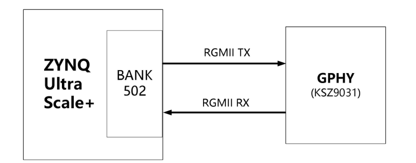
Figure 2.5.1 - ZYNQ to GPHY Connection Diagram
PS Gigabit Ethernet pin assignment is as follows:
| Signal Name | Pin Name | Pin Number | Remarks |
| PHY1_TXCK | PHY1_TXCK | AD32 | Ethernet 1 RGMII transmit clock |
| PHY1_TXD0 | PHY1_TXD0 | AE29 | Ethernet 1 transmit data bit0 |
| PHY1_TXD1 | PHY1_TXD1 | AD33 | Ethernet 1 transmit data bit1 |
| PHY1_TXD2 | PHY1_TXD2 | AE30 | Ethernet 1 transmit data bit2 |
| PHY1_TXD3 | PHY1_TXD3 | AE33 | Ethernet 1 transmit data bit3 |
| PHY1_TXCTL | PHY1_TXCTL | AE32 | Ethernet 1 transmit enable signal |
| PHY1_RXCK | PHY1_RXCK | AF30 | Ethernet 1 RGMII receive clock |
| PHY1_RXD0 | PHY1_RXD0 | AF31 | Ethernet 1 receive data Bit0 |
| PHY1_RXD1 | PHY1_RXD1 | AF32 | Ethernet 1 receive data Bit1 |
| PHY1_RXD2 | PHY1_RXD2 | AG30 | Ethernet 1 receive data Bit2 |
| PHY1_RXD3 | PHY1_RXD3 | AG33 | Ethernet 1 receive data Bit3 |
| PHY1_RXCTL | PHY1_RXCTL | AF33 | Ethernet 1 receive data valid signal |
| PHY1_MDC | PHY1_MDC | AH31 | Ethernet 1 MDIO management clock |
| PHY1_MDIO | PHY1_MDIO | AG31 | Ethernet 1 MDIO management data |
Table 2.5.2 - PS Gigabit Ethernet Pin Assignment
2.6 UART Interface
The carrier board is equipped with 2x UART-to-USB interfaces, one connected to the PS side and one to the PL side. The conversion chip uses Silicon Labs CP2102 USB-UART chip, with a Type-C USB connector. It can be connected to a PC USB port via a USB cable for serial data communication. The USB UART circuit design diagram is shown below.
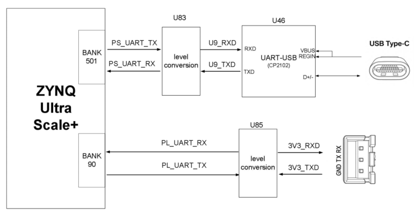
Figure 2.6.1 - USB to Serial Port Diagram
USB-to-serial ZYNQ pin assignment:
| Signal Name | Pin Name | Pin Number | Remarks |
| PS_UART_RX | PS_MIO38 | R27 | PS UART data input |
| PS_UART_TX | PS_MIO39 | P29 | PS UART data output |
| PL_UART_RX | B91_L3_N | G12 | PL UART data input |
| PL_UART_TX | B91_L3_P | H13 | PL UART data output |
Table 2.6.1 - USB to Serial Port Pin Assignment
2.7 SD Card Slot
The carrier board includes a Micro SD card interface derived from the MPSoC, providing user access to SD card storage for BOOT programs, Linux OS kernel, file system, and other user data files. The SDIO signals are connected to the ZU19EG PS BANK 501 IO signals. Since the BANK 501 VCCIO is set to 1.8V but the SD card data level is 3.3V, a TXS02612 level shifter is used for connection. The schematic of the ZU19EG PS and SD card connector is shown in the figure.
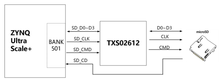
Figure 2.7.1 - SD Card Connection Diagram
SD Card Slot Pin Assignment
| Signal Name | Pin Name | Pin Number | Remarks |
| SD_CLK | PS_MIO47_501 | W30 | SD clock signal |
| SD_CD | PS_MIO45_501 | T29 | SD card detect signal |
| SD_D0 | PS_MIO46_501 | U28 | SD data Data0 |
| SD_D1 | PS_MIO47_501 | T28 | SD data Data1 |
| SD_D2 | PS_MIO48_501 | V30 | SD data Data2 |
| SD_D3 | PS_MIO49_501 | U29 | SD data Data3 |
| SD_CMD | PS_MIO50_501 | V29 | SD command signal |
Table 2.7.1 - SD Card Slot Pin Assignment
2.8 FMC Interface
The carrier board has three FMC HPC expansion ports forming a standard three-width FMC interface. FMC1 and FMC2 support various XILINX or ALINX FMC modules (HDMI input/output modules, dual-camera modules, high-speed AD modules, etc.). FMC3 operates at 3.3V and can be used with our FPGA expansion IO module (FL1010V). The FMC1 expansion port includes 72 pairs of differential IO signals (1.8V and 1.2V adjustable) and 8 pairs of GTH transceiver signals. The FMC2 expansion port includes 48 pairs of differential IO signals (1.8V and 1.2V adjustable) and 8 pairs of GTH transceiver signals. The FMC3 expansion port includes 36 pairs of differential IO signals (3.3V level) and 8 pairs of GTH transceiver signals. Due to limited FPGA pins, not all FMC expansion ports are connected to the FPGA. Not all FMC modules can be connected externally; refer to the schematic design to evaluate which modules are usable.
The FMC1 expansion port's 72 pairs of differential signals are connected to the ZYNQ UltraScale+ chip BANK 64, 65, 66 IO. The voltage level is 1.8V or 1.2V (selectable via jumper J22). The differential signals support LVDS data communication. 8 pairs of GTH transceiver signals are connected to BANK 224 and BANK 225. The schematic of the ZYNQ UltraScale+ and FMC1 connector is shown in the figure.
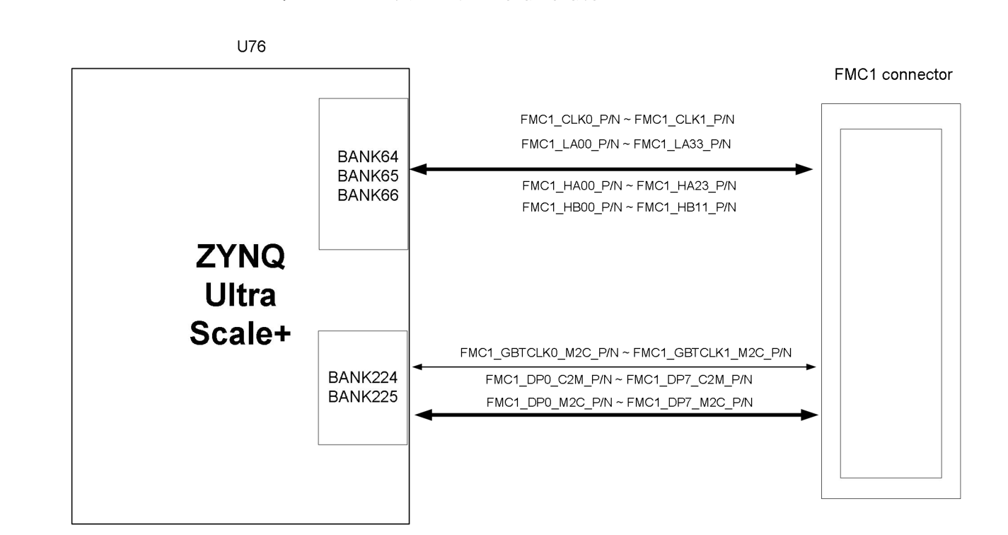
Figure 2.8.1 - FMC1 Connector Connection Diagram
FMC1 Connector Pin Assignment
| FMC1 PIN | Signal Name | Pin Name | Pin Number | Description |
| H5 | FMC1_CLK0_N | B64_L11_N | AV21 | FMC Reference 1st Clock N |
| H4 | FMC1_CLK0_P | B64_L11_P | AU21 | FMC Reference 1st Clock P |
| G3 | FMC1_CLK1_N | B64_L12_N | AV19 | FMC Reference 2nd Clock N |
| G2 | FMC1_CLK1_P | B64_L12_P | AU20 | FMC Reference 2nd Clock P |
| C3 | FMC1_DP0_C2M_N | 225_TX0_N | AR5 | FMC Transceiver Data TX0 Negative |
| C2 | FMC1_DP0_C2M_P | 225_TX0_P | AR6 | FMC Transceiver Data TX0 Positive |
| C7 | FMC1_DP0_M2C_N | 225_RX0_N | AT3 | FMC Transceiver Data RX0 Negative |
| C6 | FMC1_DP0_M2C_P | 225_RX0_P | AT4 | FMC Transceiver Data RX0 Positive |
| A23 | FMC1_DP1_C2M_N | 225_TX3_N | AM7 | FMC Transceiver Data TX1 Negative |
| A22 | FMC1_DP1_C2M_P | 225_TX3_P | AM8 | FMC Transceiver Data TX1 Positive |
| A3 | FMC1_DP1_M2C_N | 225_RX3_N | AN1 | FMC Transceiver Data RX1 Negative |
| A2 | FMC1_DP1_M2C_P | 225_RX3_P | AN2 | FMC Transceiver Data RX1 Positive |
| A27 | FMC1_DP2_C2M_N | 225_TX2_N | AN5 | FMC Transceiver Data TX2 Negative |
| A26 | FMC1_DP2_C2M_P | 225_TX2_P | AN6 | FMC Transceiver Data TX2 Positive |
| A7 | FMC1_DP2_M2C_N | 225_RX2_N | AP3 | FMC Transceiver Data RX2 Negative |
| A6 | FMC1_DP2_M2C_P | 225_RX2_P | AP4 | FMC Transceiver Data RX2 Positive |
| A31 | FMC1_DP3_C2M_N | 225_TX1_N | AP7 | FMC Transceiver Data TX3 Negative |
| A30 | FMC1_DP3_C2M_P | 225_TX1_P | AP8 | FMC Transceiver Data TX3 Positive |
| A11 | FMC1_DP3_M2C_N | 225_RX1_N | AR1 | FMC Transceiver Data RX3 Negative |
| A10 | FMC1_DP3_M2C_P | 225_RX1_P | AR2 | FMC Transceiver Data RX3 Positive |
| A35 | FMC1_DP4_C2M_N | 224_TX1_N | AW5 | FMC Transceiver Data TX4 Negative |
| A34 | FMC1_DP4_C2M_P | 224_TX1_P | AW6 | FMC Transceiver Data TX4 Positive |
| A15 | FMC1_DP4_M2C_N | 224_RX1_N | AW1 | FMC Transceiver Data RX4 Negative |
| A14 | FMC1_DP4_M2C_P | 224_RX1_P | AW2 | FMC Transceiver Data RX4 Positive |
| A39 | FMC1_DP5_C2M_N | 224_TX0_N | AY3 | FMC Transceiver Data TX5 Negative |
| A38 | FMC1_DP5_C2M_P | 224_TX0_P | AY4 | FMC Transceiver Data TX5 Positive |
| A19 | FMC1_DP5_M2C_N | 224_RX0_N | BA1 | FMC Transceiver Data RX5 Negative |
| A18 | FMC1_DP5_M2C_P | 224_RX0_P | BA2 | FMC Transceiver Data RX5 Positive |
| B37 | FMC1_DP6_C2M_N | 224_TX2_N | AU5 | FMC Transceiver Data TX6 Negative |
| B36 | FMC1_DP6_C2M_P | 224_TX2_P | AU6 | FMC Transceiver Data TX6 Positive |
| B17 | FMC1_DP6_M2C_N | 224_RX2_N | AV3 | FMC Transceiver Data RX6 Negative |
| B16 | FMC1_DP6_M2C_P | 224_RX2_P | AV4 | FMC Transceiver Data RX6 Positive |
| B33 | FMC1_DP7_C2M_N | 224_TX3_N | AT7 | FMC Transceiver Data TX7 Negative |
| B32 | FMC1_DP7_C2M_P | 224_TX3_P | AT8 | FMC Transceiver Data TX7 Positive |
| B13 | FMC1_DP7_M2C_N | 224_RX3_N | AU1 | FMC Transceiver Data RX7 Negative |
| B12 | FMC1_DP7_M2C_P | 224_RX3_P | AU2 | FMC Transceiver Data RX7 Positive |
| D5 | FMC1_GBTCLK0_M2C_N | 224_CLK1_N | AJ9 | FMC Transceiver Reference Clock 0 Negative |
| D4 | FMC1_GBTCLK0_M2C_P | 224_CLK1_P | AJ10 | FMC Transceiver Reference Clock 0 Positive |
| B21 | FMC1_GBTCLK1_M2C_N | 225_CLK1_N | AG9 | FMC Transceiver Reference Clock 1 Negative |
| B20 | FMC1_GBTCLK1_M2C_P | 225_CLK1_P | AG10 | FMC Transceiver Reference Clock 1 Positive |
| F5 | FMC1_HA00_CC_N | B66_L11_N | AW14 | FMC HA 0th Data ( Clock ) N |
| F4 | FMC1_HA00_CC_P | B66_L11_P | AW15 | FMC HA 0th Data ( Clock ) P |
| E3 | FMC1_HA01_CC_N | B66_L12_N | AV14 | FMC HA 1st Data ( Clock ) N |
| E2 | FMC1_HA01_CC_P | B66_L12_P | AU14 | FMC HA 1st Data ( Clock ) P |
| K8 | FMC1_HA02_N | B66_L10_N | AV13 | FMC HA 2nd Data N |
| K7 | FMC1_HA02_P | B66_L10_P | AU13 | FMC HA 2nd Data P |
| J7 | FMC1_HA03_N | B66_L22_N | AK17 | FMC HA 3rd Data N |
| J6 | FMC1_HA03_P | B66_L22_P | AJ17 | FMC HA 3rd Data P |
| F8 | FMC1_HA04_N | B66_L24_N | AP16 | FMC HA 4th Data N |
| F7 | FMC1_HA04_P | B66_L24_P | AN16 | FMC HA 4th Data P |
| E7 | FMC1_HA05_N | B66_L19_N | AK18 | FMC HA 5th Data N |
| E6 | FMC1_HA05_P | B66_L19_P | AJ18 | FMC HA 5th Data P |
| K11 | FMC1_HA06_N | B66_L8_N | BB11 | FMC HA 6th Data N |
| K10 | FMC1_HA06_P | B66_L8_P | BA11 | FMC HA 6th Data P |
| J10 | FMC1_HA07_N | B66_L7_N | BA12 | FMC HA 7th Data N |
| J9 | FMC1_HA07_P | B66_L7_P | AY12 | FMC HA 7th Data P |
| F11 | FMC1_HA08_N | B66_L5_N | AY14 | FMC HA 8th Data N |
| F10 | FMC1_HA08_P | B66_L5_P | AY15 | FMC HA 8th Data P |
| E10 | FMC1_HA09_N | B66_L17_N | AT17 | FMC HA 9th Data N |
| E9 | FMC1_HA09_P | B66_L17_P | AR17 | FMC HA 9th Data P |
| K14 | FMC1_HA10_N | B66_L1_N | BA17 | FMC HA 10th Data N |
| K13 | FMC1_HA10_P | B66_L1_P | AY17 | FMC HA 10th Data P |
| J13 | FMC1_HA11_N | B66_L13_N | AV16 | FMC HA 11th Data N |
| J12 | FMC1_HA11_P | B66_L13_P | AV17 | FMC HA 11th Data P |
| F14 | FMC1_HA12_N | B66_L6_N | BB13 | FMC HA 12th Data N |
| F13 | FMC1_HA12_P | B66_L6_P | BA13 | FMC HA 12th Data P |
| E13 | FMC1_HA13_N | B66_L3_N | AW16 | FMC HA 13th Data N |
| E12 | FMC1_HA13_P | B66_L3_P | AW17 | FMC HA 13th Data P |
| J16 | FMC1_HA14_N | B66_L9_N | BB10 | FMC HA 14th Data N |
| J15 | FMC1_HA14_P | B66_L9_P | BA10 | FMC HA 14th Data P |
| F17 | FMC1_HA15_N | B66_L23_N | AM16 | FMC HA 15th Data N |
| F16 | FMC1_HA15_P | B66_L23_P | AL16 | FMC HA 15th Data P |
| E16 | FMC1_HA16_N | B66_L18_N | AU16 | FMC HA 16th Data N |
| E15 | FMC1_HA16_P | B66_L18_P | AT16 | FMC HA 16th Data P |
| K17 | FMC1_HA17_CC_N | B66_L14_N | AU15 | FMC HA 17th Data ( Clock ) N |
| K16 | FMC1_HA17_CC_P | B66_L14_P | AT15 | FMC HA 17th Data ( Clock ) P |
| J19 | FMC1_HA18_N | B66_L21_N | AN17 | FMC HA 18th Data N |
| J18 | FMC1_HA18_P | B66_L21_P | AN18 | FMC HA 18th Data P |
| F20 | FMC1_HA19_N | B66_L2_N | BB16 | FMC HA 19th Data N |
| F19 | FMC1_HA19_P | B66_L2_P | BA16 | FMC HA 19th Data P |
| E19 | FMC1_HA20_N | B66_L20_N | AM18 | FMC HA 20th Data N |
| E18 | FMC1_HA20_P | B66_L20_P | AL18 | FMC HA 20th Data P |
| K20 | FMC1_HA21_N | B66_L16_N | AT18 | FMC HA 21st Data N |
| K19 | FMC1_HA21_P | B66_L16_P | AR18 | FMC HA 21st Data P |
| J22 | FMC1_HA22_N | B66_L15_N | AV18 | FMC HA 22nd Data N |
| J21 | FMC1_HA22_P | B66_L15_P | AU18 | FMC HA 22nd Data P |
| K23 | FMC1_HA23_N | B66_L4_N | BB15 | FMC HA 23rd Data N |
| K22 | FMC1_HA23_P | B66_L4_P | BA15 | FMC HA 23rd Data P |
| K26 | FMC1_HB00_CC_N | B64_L6_N | BB18 | FMC HB 0th Data ( Clock ) N |
| K25 | FMC1_HB00_CC_P | B64_L6_P | BA18 | FMC HB 0th Data ( Clock ) P |
| J25 | FMC1_HB01_N | B64_L7_N | AV23 | FMC HB 1st Data N |
| J24 | FMC1_HB01_P | B64_L7_P | AU23 | FMC HB 1st Data P |
| F23 | FMC1_HB02_N | B64_L10_N | AY18 | FMC HB 2nd Data N |
| F22 | FMC1_HB02_P | B64_L10_P | AY19 | FMC HB 2nd Data P |
| E22 | FMC1_HB03_N | B64_L9_N | AW19 | FMC HB 3rd Data N |
| E21 | FMC1_HB03_P | B64_L9_P | AW20 | FMC HB 3rd Data P |
| F26 | FMC1_HB04_N | B65_L19_N | AT23 | FMC HB 4th Data N |
| F25 | FMC1_HB04_P | B65_L19_P | AR23 | FMC HB 4th Data P |
| E25 | FMC1_HB05_N | B64_L24_N | AK22 | FMC HB 5th Data N |
| E24 | FMC1_HB05_P | B64_L24_P | AJ22 | FMC HB 5th Data P |
| K29 | FMC1_HB06_CC_N | B65_L21_N | AN24 | FMC HB 6th Data ( Clock ) N |
| K28 | FMC1_HB06_CC_P | B65_L21_P | AM24 | FMC HB 6th Data ( Clock ) P |
| J28 | FMC1_HB07_N | B65_L20_N | AP25 | FMC HB 7th Data N |
| J27 | FMC1_HB07_P | B65_L20_P | AP24 | FMC HB 7th Data P |
| F29 | FMC1_HB08_N | B65_L22_N | AN23 | FMC HB 8th Data N |
| F28 | FMC1_HB08_P | B65_L22_P | AM23 | FMC HA 8th Data P |
| E28 | FMC1_HB09_N | B65_L6_N | BB28 | FMC HB 9th Data N |
| E27 | FMC1_HB09_P | B65_L6_P | BA28 | FMC HB 9th Data P |
| K32 | FMC1_HB10_N | B65_L18_N | AT28 | FMC HB 10th Data N |
| K31 | FMC1_HB10_P | B65_L18_P | AR28 | FMC HB 10th Data P |
| J31 | FMC1_HB11_N | B65_L23_N | AL23 | FMC HB 11th Data N |
| J30 | FMC1_HB11_P | B65_L23_P | AK23 | FMC HA 11th Data P |
| G7 | FMC1_LA00_CC_N | B64_L13_N | AT21 | FMC LA 0th Data ( Clock ) N |
| G6 | FMC1_LA00_CC_P | B64_L13_P | AT22 | FMC LA 0th Data ( Clock ) P |
| D9 | FMC1_LA01_CC_N | B64_L14_N | AU19 | FMC LA 1st Data ( Clock ) N |
| D8 | FMC1_LA01_CC_P | B64_L14_P | AT20 | FMC LA 1st Data ( Clock ) P |
| H8 | FMC1_LA02_N | B64_L18_N | AR19 | FMC LA 2nd Data N |
| H7 | FMC1_LA02_P | B64_L18_P | AP19 | FMC LA 2nd Data P |
| G10 | FMC1_LA03_N | B64_L8_N | AW22 | FMC LA 3rd Data N |
| G9 | FMC1_LA03_P | B64_L8_P | AV22 | FMC LA 3rd Data P |
| H11 | FMC1_LA04_N | B64_L16_N | AP21 | FMC LA 4th Data N |
| H10 | FMC1_LA04_P | B64_L16_P | AN21 | FMC LA 4th Data P |
| D12 | FMC1_LA05_N | B64_L15_N | AP22 | FMC LA 5th Data N |
| D11 | FMC1_LA05_P | B64_L15_P | AN22 | FMC LA 5th Data P |
| C11 | FMC1_LA06_N | B64_L21_N | AL21 | FMC LA 6th Data N |
| C10 | FMC1_LA06_P | B64_L21_P | AL22 | FMC LA 6th Data P |
| H14 | FMC1_LA07_N | B64_L20_N | AM20 | FMC LA 7th Data N |
| H13 | FMC1_LA07_P | B64_L20_P | AM21 | FMC LA 7th Data P |
| G13 | FMC1_LA08_N | B64_L23_N | AJ20 | FMC LA 8th Data N |
| G12 | FMC1_LA08_P | B64_L23_P | AJ21 | FMC LA 8th Data P |
| D15 | FMC1_LA09_N | B64_L22_N | AK19 | FMC LA 9th Data N |
| D14 | FMC1_LA09_P | B64_L22_P | AK20 | FMC LA 9th Data P |
| C15 | FMC1_LA10_N | B64_L17_N | AR20 | FMC LA 10th Data N |
| C14 | FMC1_LA10_P | B64_L17_P | AP20 | FMC LA 10th Data P |
| H17 | FMC1_LA11_N | B64_L5_N | BB19 | FMC LA 11th Data N |
| H16 | FMC1_LA11_P | B64_L5_P | BB20 | FMC LA 11th Data P |
| G16 | FMC1_LA12_N | B64_L19_N | AN19 | FMC LA 12th Data N |
| G15 | FMC1_LA12_P | B64_L19_P | AM19 | FMC LA 12th Data P |
| D18 | FMC1_LA13_N | B64_L2_N | AY22 | FMC LA 13th Data N |
| D17 | FMC1_LA13_P | B64_L2_P | AY23 | FMC LA 13th Data P |
| C19 | FMC1_LA14_N | B64_L1_N | BB23 | FMC LA 14th Data N |
| C18 | FMC1_LA14_P | B64_L1_P | BA23 | FMC LA 14th Data P |
| H20 | FMC1_LA15_N | B64_L4_N | BA20 | FMC LA 15th Data N |
| H19 | FMC1_LA15_P | B64_L4_P | AY20 | FMC LA 15th Data P |
| G19 | FMC1_LA16_N | B64_L3_N | BA21 | FMC LA 16th Data N |
| G18 | FMC1_LA16_P | B64_L3_P | BA22 | FMC LA 16th Data P |
| D21 | FMC1_LA17_CC_N | B65_L14_N | AR25 | FMC LA 17th Data ( Clock ) N |
| D20 | FMC1_LA17_CC_P | B65_L14_P | AR24 | FMC LA 17th Data ( Clock ) P |
| C23 | FMC1_LA18_CC_N | B65_L13_N | AT27 | FMC LA 18th Data ( Clock ) N |
| C22 | FMC1_LA18_CC_P | B65_L13_P | AR27 | FMC LA 18th Data ( Clock ) P |
| H23 | FMC1_LA19_N | B65_L12_N | AT26 | FMC LA 19th Data N |
| H22 | FMC1_LA19_P | B65_L12_P | AT25 | FMC LA 19th Data P |
| G22 | FMC1_LA20_N | B65_L17_N | AN28 | FMC LA 20th Data N |
| G21 | FMC1_LA20_P | B65_L17_P | AM28 | FMC LA 20th Data P |
| H26 | FMC1_LA21_N | B65_L2_N | BB25 | FMC LA 21st Data N |
| H25 | FMC1_LA21_P | B65_L2_P | BB24 | FMC LA 21st Data P |
| G25 | FMC1_LA22_N | B65_L5_N | AY28 | FMC LA 22nd Data N |
| G24 | FMC1_LA22_P | B65_L5_P | AY27 | FMC LA 22nd Data P |
| D24 | FMC1_LA23_N | B65_L4_N | BB26 | FMC LA 23rd Data N |
| D23 | FMC1_LA23_P | B65_L4_P | BA26 | FMC LA 23rd Data P |
| H29 | FMC1_LA24_N | B65_L16_N | AP27 | FMC LA 24th Data N |
| H28 | FMC1_LA24_P | B65_L16_P | AN27 | FMC LA 24th Data P |
| G28 | FMC1_LA25_N | B65_L24_N | AK24 | FMC LA 25th Data N |
| G27 | FMC1_LA25_P | B65_L24_P | AJ24 | FMC LA 25th Data P |
| D27 | FMC1_LA26_N | B65_L1_N | AY24 | FMC LA 26th Data N |
| D26 | FMC1_LA26_P | B65_L1_P | AW24 | FMC LA 26th Data P |
| C27 | FMC1_LA27_N | B65_L3_N | BA25 | FMC LA 27th Data N |
| C26 | FMC1_LA27_P | B65_L3_P | AY25 | FMC LA 27th Data P |
| H32 | FMC1_LA28_N | B65_L15_N | AN26 | FMC LA 28th Data N |
| H31 | FMC1_LA28_P | B65_L15_P | AM26 | FMC LA 28th Data P |
| G31 | FMC1_LA29_N | B65_L7_N | AV24 | FMC LA 29th Data N |
| G30 | FMC1_LA29_P | B65_L7_P | AU24 | FMC LA 29th Data P |
| H35 | FMC1_LA30_N | B65_L8_N | AW26 | FMC LA 30th Data N |
| H34 | FMC1_LA30_P | B65_L8_P | AV26 | FMC LA 30th Data P |
| G34 | FMC1_LA31_N | B65_L10_N | AV28 | FMC LA 31st Data N |
| G33 | FMC1_LA31_P | B65_L10_P | AU28 | FMC LA 31st Data P |
| H38 | FMC1_LA32_N | B65_L9_N | AW27 | FMC LA 32nd Data N |
| H37 | FMC1_LA32_P | B65_L9_P | AV27 | FMC LA 32nd Data P |
| G37 | FMC1_LA33_N | B65_L11_N | AU26 | FMC LA 33rd Data N |
| G36 | FMC1_LA33_P | B65_L11_P | AU25 | FMC LA 33rd Data P |
Table 2.8.1 - FMC1 Connector Pin Assignment
The FMC2 expansion port's 42 pairs of differential signals are connected to the ZYNQ UltraScale+ chip BANK 67, 68 IO. The voltage level is 1.8V or 1.2V (selectable via jumper J51). The differential signals support LVDS data communication. 8 pairs of GTH transceiver signals are connected to BANK 228 and BANK 229. The schematic of the ZYNQ UltraScale+ and FMC2 connector is shown below.
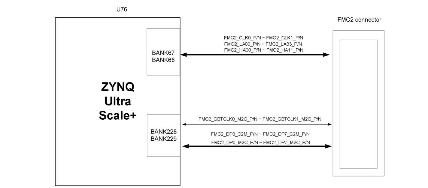
Figure 2.8.2 - FMC2 Connector Connection Diagram
FMC2 Connector Pin Assignment
| FMC2 PIN | Signal Name | ZYNQ Pin Name | ZYNQ Pin Number | Description |
| H5 | FMC2_CLK0_M2C_N | B68_L12_N | F15 | FMC Reference 1st Clock N |
| H4 | FMC2_CLK0_M2C_P | B68_L12_P | G16 | FMC Reference 1st Clock P |
| G3 | FMC2_CLK1_M2C_N | B68_L11_N | F17 | FMC Reference 2nd Clock N |
| G2 | FMC2_CLK1_M2C_P | B68_L11_P | G17 | FMC Reference 2nd Clock P |
| C3 | FMC2_DP0_C2M_N | 229_TX1_N | V7 | FMC Transceiver Data TX0 Negative |
| C2 | FMC2_DP0_C2M_P | 229_TX1_P | V8 | FMC Transceiver Data TX0 Positive |
| C7 | FMC2_DP0_M2C_N | 229_RX1_N | W1 | FMC Transceiver Data RX0 Negative |
| C6 | FMC2_DP0_M2C_P | 229_RX1_P | W2 | FMC Transceiver Data RX0 Positive |
| A23 | FMC2_DP1_C2M_N | 229_TX3_N | T7 | FMC Transceiver Data TX1 Negative |
| A22 | FMC2_DP1_C2M_P | 229_TX3_P | T8 | FMC Transceiver Data TX1 Positive |
| A3 | FMC2_DP1_M2C_N | 229_RX3_N | U1 | FMC Transceiver Data RX1 Negative |
| A2 | FMC2_DP1_M2C_P | 229_RX3_P | U2 | FMC Transceiver Data RX1 Positive |
| A27 | FMC2_DP2_C2M_N | 229_TX2_N | U5 | FMC Transceiver Data TX2 Negative |
| A26 | FMC2_DP2_C2M_P | 229_TX2_P | U6 | FMC Transceiver Data TX2 Positive |
| A7 | FMC2_DP2_M2C_N | 229_RX2_N | V3 | FMC Transceiver Data RX2 Negative |
| A6 | FMC2_DP2_M2C_P | 229_RX2_P | V4 | FMC Transceiver Data RX2 Positive |
| A31 | FMC2_DP3_C2M_N | 229_TX0_N | W5 | FMC Transceiver Data TX3 Negative |
| A30 | FMC2_DP3_C2M_P | 229_TX0_P | W6 | FMC Transceiver Data TX3 Positive |
| A11 | FMC2_DP3_M2C_N | 229_RX0_N | Y3 | FMC Transceiver Data RX3 Negative |
| A10 | FMC2_DP3_M2C_P | 229_RX0_P | Y4 | FMC Transceiver Data RX3 Positive |
| A35 | FMC2_DP4_C2M_N | 228_TX2_N | AA5 | FMC Transceiver Data TX4 Negative |
| A34 | FMC2_DP4_C2M_P | 228_TX2_P | AA6 | FMC Transceiver Data TX4 Positive |
| A15 | FMC2_DP4_M2C_N | 228_RX2_N | AB3 | FMC Transceiver Data RX4 Negative |
| A14 | FMC2_DP4_M2C_P | 228_RX2_P | AB4 | FMC Transceiver Data RX4 Positive |
| A39 | FMC2_DP5_C2M_N | 228_TX0_N | AC5 | FMC Transceiver Data TX5 Negative |
| A38 | FMC2_DP5_C2M_P | 228_TX0_P | AC6 | FMC Transceiver Data TX5 Positive |
| A19 | FMC2_DP5_M2C_N | 228_RX0_N | AD3 | FMC Transceiver Data RX5 Negative |
| A18 | FMC2_DP5_M2C_P | 228_RX0_P | AD4 | FMC Transceiver Data RX5 Positive |
| B37 | FMC2_DP6_C2M_N | 228_TX1_N | AB7 | FMC Transceiver Data TX6 Negative |
| B36 | FMC2_DP6_C2M_P | 228_TX1_P | AB8 | FMC Transceiver Data TX6 Positive |
| B17 | FMC2_DP6_M2C_N | 228_RX1_N | AC1 | FMC Transceiver Data RX6 Negative |
| B16 | FMC2_DP6_M2C_P | 228_RX1_P | AC2 | FMC Transceiver Data RX6 Positive |
| B33 | FMC2_DP7_C2M_N | 228_TX3_N | Y7 | FMC Transceiver Data TX7 Negative |
| B32 | FMC2_DP7_C2M_P | 228_TX3_P | Y8 | FMC Transceiver Data TX7 Positive |
| B13 | FMC2_DP7_M2C_N | 228_RX3_N | AA1 | FMC Transceiver Data RX7 Negative |
| B12 | FMC2_DP7_M2C_P | 228_RX3_P | AA2 | FMC Transceiver Data RX7 Positive |
| D5 | FMC2_GBTCLK0_M2C_N | 228_CLK0_N | AB11 | FMC Transceiver Reference Clock 0 Negative |
| D4 | FMC2_GBTCLK0_M2C_P | 228_CLK0_P | AB12 | FMC Transceiver Reference Clock 0 Positive |
| B21 | FMC2_GBTCLK1_M2C_N | 229_CLK0_N | Y11 | FMC Transceiver Reference Clock 1 Negative |
| B20 | FMC2_GBTCLK1_M2C_P | 229_CLK0_P | Y12 | FMC Transceiver Reference Clock 1 Positive |
| F5 | FMC2_HA00_CC_N | B68_L16_N | A12 | FMC HA 0th Data ( Clock ) N |
| F4 | FMC2_HA00_CC_P | B68_L16_P | B13 | FMC HA 0th Data ( Clock ) P |
| E3 | FMC2_HA01_CC_N | B68_L17_N | A13 | FMC HA 1st Data ( Clock ) N |
| E2 | FMC2_HA01_CC_P | B68_L17_P | A14 | FMC HA 1st Data ( Clock ) P |
| K8 | FMC2_HA02_N | B68_L15_N | C13 | FMC HA 2nd Data N |
| K7 | FMC2_HA02_P | B68_L15_P | D13 | FMC HA 2nd Data P |
| J7 | FMC2_HA03_N | B68_L24_N | A18 | FMC HA 3rd Data N |
| J6 | FMC2_HA03_P | B68_L24_P | B18 | FMC HA 3rd Data P |
| F8 | FMC2_HA04_N | B67_L6_N | BB4 | FMC HA 4th Data N |
| F7 | FMC2_HA04_P | B67_L6_P | BB5 | FMC HA 4th Data P |
| E7 | FMC2_HA05_N | B68_L10_N | F18 | FMC HA 5th Data N |
| E6 | FMC2_HA05_P | B68_L10_P | G18 | FMC HA 5th Data P |
| K11 | FMC2_HA06_N | B67_L10_N | AV8 | FMC HA 6th Data N |
| K10 | FMC2_HA06_P | B67_L10_P | AV9 | FMC HA 6th Data P |
| J10 | FMC2_HA07_N | B67_L18_N | AN10 | FMC HA 7th Data N |
| J9 | FMC2_HA07_P | B67_L18_P | AM10 | FMC HA 7th Data P |
| F11 | FMC2_HA08_N | B67_L8_N | AV11 | FMC HA 8th Data N |
| F10 | FMC2_HA08_P | B67_L8_P | AU11 | FMC HA 8th Data P |
| E10 | FMC2_HA09_N | B67_L24_N | AK14 | FMC HA 9th Data N |
| E9 | FMC2_HA09_P | B67_L24_P | AJ14 | FMC HA 9th Data P |
| K14 | FMC2_HA10_N | B67_L9_N | AW10 | FMC HA 10th Data N |
| K13 | FMC2_HA10_P | B67_L9_P | AW11 | FMC HA 10th Data P |
| J13 | FMC2_HA11_N | B67_L11_N | AT12 | FMC HA 11th Data N |
| J12 | FMC2_HA11_P | B67_L11_P | AT13 | FMC HA 11th Data P |
| G7 | FMC2_LA00_CC_N | B68_L13_N | E14 | FMC LA 0th Data ( Clock ) N |
| G6 | FMC2_LA00_CC_P | B68_L13_P | F14 | FMC LA 0th Data ( Clock ) P |
| D9 | FMC2_LA01_CC_N | B68_L14_N | D14 | FMC LA 1st Data ( Clock ) N |
| D8 | FMC2_LA01_CC_P | B68_L14_P | E15 | FMC LA 1st Data ( Clock ) P |
| H8 | FMC2_LA02_N | B68_L18_N | B15 | FMC LA 2nd Data N |
| H7 | FMC2_LA02_P | B68_L18_P | C15 | FMC LA 2nd Data P |
| G10 | FMC2_LA03_N | B68_L7_N | G15 | FMC LA 3rd Data N |
| G9 | FMC2_LA03_P | B68_L7_P | H15 | FMC LA 3rd Data P |
| H11 | FMC2_LA04_N | B68_L8_N | H16 | FMC LA 4th Data N |
| H10 | FMC2_LA04_P | B68_L8_P | J16 | FMC LA 4th Data P |
| D12 | FMC2_LA05_N | B68_L6_N | K17 | FMC LA 5th Data N |
| D11 | FMC2_LA05_P | B68_L6_P | L17 | FMC LA 5th Data P |
| C11 | FMC2_LA06_N | B68_L20_N | B16 | FMC LA 6th Data N |
| C10 | FMC2_LA06_P | B68_L20_P | C16 | FMC LA 6th Data P |
| H14 | FMC2_LA07_N | B68_L21_N | D17 | FMC LA 7th Data N |
| H13 | FMC2_LA07_P | B68_L21_P | E17 | FMC LA 7th Data P |
| G13 | FMC2_LA08_N | B68_L22_N | A17 | FMC LA 8th Data N |
| G12 | FMC2_LA08_P | B68_L22_P | B17 | FMC LA 8th Data P |
| D15 | FMC2_LA09_N | B68_L23_N | C18 | FMC LA 9th Data N |
| D14 | FMC2_LA09_P | B68_L23_P | D18 | FMC LA 9th Data P |
| C15 | FMC2_LA10_N | B68_L9_N | H18 | FMC LA 10th Data N |
| C14 | FMC2_LA10_P | B68_L9_P | J18 | FMC LA 10th Data P |
| H17 | FMC2_LA11_N | B68_L5_N | K15 | FMC LA 11th Data N |
| H16 | FMC2_LA11_P | B68_L5_P | K16 | FMC LA 11th Data P |
| G16 | FMC2_LA12_N | B68_L19_N | D16 | FMC LA 12th Data N |
| G15 | FMC2_LA12_P | B68_L19_P | E16 | FMC LA 12th Data P |
| D18 | FMC2_LA13_N | B68_L3_N | M16 | FMC LA 13th Data N |
| D17 | FMC2_LA13_P | B68_L3_P | M17 | FMC LA 13th Data P |
| C19 | FMC2_LA14_N | B68_L1_N | N15 | FMC LA 14th Data N |
| C18 | FMC2_LA14_P | B68_L1_P | P15 | FMC LA 14th Data P |
| H20 | FMC2_LA15_N | B68_L2_N | N16 | FMC LA 15th Data N |
| H19 | FMC2_LA15_P | B68_L2_P | P16 | FMC LA 15th Data P |
| G19 | FMC2_LA16_N | B68_L4_N | L15 | FMC LA 16th Data N |
| G18 | FMC2_LA16_P | B68_L4_P | M15 | FMC LA 16th Data P |
| D21 | FMC2_LA17_CC_N | B67_L14_N | AR10 | FMC LA 17th Data ( Clock ) N |
| D20 | FMC2_LA17_CC_P | B67_L14_P | AP10 | FMC LA 17th Data ( Clock ) P |
| C23 | FMC2_LA18_CC_N | B67_L13_N | AR12 | FMC LA 18th Data ( Clock ) N |
| C22 | FMC2_LA18_CC_P | B67_L13_P | AR13 | FMC LA 18th Data ( Clock ) P |
| H23 | FMC2_LA19_N | B67_L12_N | AT10 | FMC LA 19th Data N |
| H22 | FMC2_LA19_P | B67_L12_P | AT11 | FMC LA 19th Data P |
| G22 | FMC2_LA20_N | B67_L17_N | AN11 | FMC LA 20th Data N |
| G21 | FMC2_LA20_P | B67_L17_P | AM11 | FMC LA 20th Data P |
| H26 | FMC2_LA21_N | B67_L5_N | BB6 | FMC LA 21st Data N |
| H25 | FMC2_LA21_P | B67_L5_P | BA6 | FMC LA 21st Data P |
| G25 | FMC2_LA22_N | B67_L2_N | BB8 | FMC LA 22nd Data N |
| G24 | FMC2_LA22_P | B67_L2_P | BB9 | FMC LA 22nd Data P |
| D24 | FMC2_LA23_N | B67_L4_N | BA7 | FMC LA 23rd Data N |
| D23 | FMC2_LA23_P | B67_L4_P | BA8 | FMC LA 23rd Data P |
| H29 | FMC2_LA24_N | B67_L16_N | AP12 | FMC LA 24th Data N |
| H28 | FMC2_LA24_P | B67_L16_P | AN12 | FMC LA 24th Data P |
| G28 | FMC2_LA25_N | B67_L7_N | AW12 | FMC LA 25th Data N |
| G27 | FMC2_LA25_P | B67_L7_P | AV12 | FMC LA 25th Data P |
| D27 | FMC2_LA26_N | B67_L1_N | AY9 | FMC LA 26th Data N |
| D26 | FMC2_LA26_P | B67_L1_P | AW9 | FMC LA 26th Data P |
| C27 | FMC2_LA27_N | B67_L3_N | AY8 | FMC LA 27th Data N |
| C26 | FMC2_LA27_P | B67_L3_P | AW8 | FMC LA 27th Data P |
| H32 | FMC2_LA28_N | B67_L15_N | AR14 | FMC LA 28th Data N |
| H31 | FMC2_LA28_P | B67_L15_P | AR15 | FMC LA 28th Data P |
| G31 | FMC2_LA29_N | B67_L19_N | AM15 | FMC LA 29th Data N |
| G30 | FMC2_LA29_P | B67_L19_P | AL15 | FMC LA 29th Data P |
| H35 | FMC2_LA30_N | B67_L22_N | AP14 | FMC LA 30th Data N |
| H34 | FMC2_LA30_P | B67_L22_P | AN14 | FMC LA 30th Data P |
| G34 | FMC2_LA31_N | B67_L21_N | AM14 | FMC LA 31st Data N |
| G33 | FMC2_LA31_P | B67_L21_P | AL14 | FMC LA 31st Data P |
| H38 | FMC2_LA32_N | B67_L23_N | AN13 | FMC LA 32nd Data N |
| H37 | FMC2_LA32_P | B67_L23_P | AM13 | FMC LA 32nd Data P |
| G37 | FMC2_LA33_N | B67_L20_N | AK15 | FMC LA 33rd Data N |
| G36 | FMC2_LA33_P | B67_L20_P | AJ15 | FMC LA 33rd Data P |
Table 2.8.2 - FMC2 Connector Pin Assignment
The FMC3 expansion port's 42 pairs of differential signals are connected to the ZYNQ UltraScale+ chip BANK 90, 93, 94 IO at 3.3V voltage level. FPGA expansion IO ports can be derived through FMC modules. 8 pairs of GTH transceiver signals are connected to BANK 228 and BANK 229. The schematic of the ZYNQ UltraScale+ and FMC3 connector is shown below.
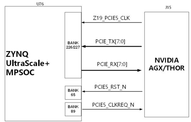
Figure 2.8.3 - FMC3 Connector Connection Diagram
FMC3 Connector Pin Assignment
| FMC3PIN | Signal Name | ZYNQ Pin Name | ZYNQ Pin Number | Description |
| H5 | FMC3_CLK0_M2C_N | B94_L8_N | C3 | FMC Reference 1st Clock N |
| H4 | FMC3_CLK0_M2C_P | B94_L8_P | C4 | FMC Reference 1st Clock P |
| G3 | FMC3_CLK1_M2C_N | B94_L5_N | D3 | FMC Reference 2nd Clock N |
| G2 | FMC3_CLK1_M2C_P | B94_L5_P | D4 | FMC Reference 2nd Clock P |
| C3 | FMC3_DP0_C2M_N | 231_TX1_N | K3 | FMC Transceiver Data TX0 Negative |
| C2 | FMC3_DP0_C2M_P | 231_TX1_P | K4 | FMC Transceiver Data TX0 Positive |
| C7 | FMC3_DP0_M2C_N | 231_RX1_N | L1 | FMC Transceiver Data RX0 Negative |
| C6 | FMC3_DP0_M2C_P | 231_RX1_P | L2 | FMC Transceiver Data RX0 Positive |
| A23 | FMC3_DP1_C2M_N | 231_TX3_N | H3 | FMC Transceiver Data TX1 Negative |
| A22 | FMC3_DP1_C2M_P | 231_TX3_P | H4 | FMC Transceiver Data TX1 Positive |
| A3 | FMC3_DP1_M2C_N | 231_RX3_N | G1 | FMC Transceiver Data RX1 Negative |
| A2 | FMC3_DP1_M2C_P | 231_RX3_P | G2 | FMC Transceiver Data RX1 Positive |
| A27 | FMC3_DP2_C2M_N | 231_TX2_N | J5 | FMC Transceiver Data TX2 Negative |
| A26 | FMC3_DP2_C2M_P | 231_TX2_P | J6 | FMC Transceiver Data TX2 Positive |
| A7 | FMC3_DP2_M2C_N | 231_RX2_N | J1 | FMC Transceiver Data RX2 Negative |
| A6 | FMC3_DP2_M2C_P | 231_RX2_P | J2 | FMC Transceiver Data RX2 Positive |
| A31 | FMC3_DP3_C2M_N | 231_TX0_N | L5 | FMC Transceiver Data TX3 Negative |
| A30 | FMC3_DP3_C2M_P | 231_TX0_P | L6 | FMC Transceiver Data TX3 Positive |
| A11 | FMC3_DP3_M2C_N | 231_RX0_N | M3 | FMC Transceiver Data RX3 Negative |
| A10 | FMC3_DP3_M2C_P | 231_RX0_P | M4 | FMC Transceiver Data RX3 Positive |
| A35 | FMC3_DP4_C2M_N | 230_TX2_N | N5 | FMC Transceiver Data TX4 Negative |
| A34 | FMC3_DP4_C2M_P | 230_TX2_P | N6 | FMC Transceiver Data TX4 Positive |
| A15 | FMC3_DP4_M2C_N | 230_RX2_N | P3 | FMC Transceiver Data RX4 Negative |
| A14 | FMC3_DP4_M2C_P | 230_RX2_P | P4 | FMC Transceiver Data RX4 Positive |
| A39 | FMC3_DP5_C2M_N | 230_TX0_N | R5 | FMC Transceiver Data TX5 Negative |
| A38 | FMC3_DP5_C2M_P | 230_TX0_P | R6 | FMC Transceiver Data TX5 Positive |
| A19 | FMC3_DP5_M2C_N | 230_RX0_N | T3 | FMC Transceiver Data RX5 Negative |
| A18 | FMC3_DP5_M2C_P | 230_RX0_P | T4 | FMC Transceiver Data RX5 Positive |
| B37 | FMC3_DP6_C2M_N | 230_TX1_N | P7 | FMC Transceiver Data TX6 Negative |
| B36 | FMC3_DP6_C2M_P | 230_TX1_P | P8 | FMC Transceiver Data TX6 Positive |
| B17 | FMC3_DP6_M2C_N | 230_RX1_N | R1 | FMC Transceiver Data RX6 Negative |
| B16 | FMC3_DP6_M2C_P | 230_RX1_P | R2 | FMC Transceiver Data RX6 Positive |
| B33 | FMC3_DP7_C2M_N | 230_TX3_N | M7 | FMC Transceiver Data TX7 Negative |
| B32 | FMC3_DP7_C2M_P | 230_TX3_P | M8 | FMC Transceiver Data TX7 Positive |
| B13 | FMC3_DP7_M2C_N | 230_RX3_N | N1 | FMC Transceiver Data RX7 Negative |
| B12 | FMC3_DP7_M2C_P | 230_RX3_P | N2 | FMC Transceiver Data RX7 Positive |
| D5 | FMC3_GBTCLK0_M2C_N | 230_CLK1_N | U9 | FMC Transceiver Reference Clock 0 Negative |
| D4 | FMC3_GBTCLK0_M2C_P | 230_CLK1_P | U10 | FMC Transceiver Reference Clock 0 Positive |
| B21 | FMC3_GBTCLK1_M2C_N | 231_CLK1_N | R9 | FMC Transceiver Reference Clock 1 Negative |
| B20 | FMC3_GBTCLK1_M2C_P | 231_CLK1_P | R10 | FMC Transceiver Reference Clock 1 Positive |
| G7 | FMC3_LA00_CC_N | B90_L6_N | M11 | FMC LA 0th Data ( Clock ) N |
| G6 | FMC3_LA00_CC_P | B90_L6_P | M12 | FMC LA 0th Data ( Clock ) P |
| D9 | FMC3_LA01_CC_N | B90_L5_N | M13 | FMC LA 1st Data ( Clock ) N |
| D8 | FMC3_LA01_CC_P | B90_L5_P | N13 | FMC LA 1st Data ( Clock ) P |
| H8 | FMC3_LA02_N | B90_L1_N | N10 | FMC LA 2nd Data N |
| H7 | FMC3_LA02_P | B90_L1_P | N11 | FMC LA 2nd Data P |
| G10 | FMC3_LA03_N | B90_L9_N | L10 | FMC LA 3rd Data N |
| G9 | FMC3_LA03_P | B90_L9_P | M10 | FMC LA 3rd Data P |
| H11 | FMC3_LA04_N | B90_L2_N | N12 | FMC LA 4th Data N |
| H10 | FMC3_LA04_P | B90_L2_P | P12 | FMC LA 4th Data P |
| D12 | FMC3_LA05_N | B90_L3_N | P13 | FMC LA 5th Data N |
| D11 | FMC3_LA05_P | B90_L3_P | R14 | FMC LA 5th Data P |
| C11 | FMC3_LA06_N | B90_L4_N | N14 | FMC LA 6th Data N |
| C10 | FMC3_LA06_P | B90_L4_P | P14 | FMC LA 6th Data P |
| H14 | FMC3_LA07_N | B90_L11_N | J14 | FMC LA 7th Data N |
| H13 | FMC3_LA07_P | B90_L11_P | K14 | FMC LA 7th Data P |
| G13 | FMC3_LA08_N | B90_L8_N | L13 | FMC LA 8th Data N |
| G12 | FMC3_LA08_P | B90_L8_P | L14 | FMC LA 8th Data P |
| D15 | FMC3_LA09_N | B90_L10_N | K10 | FMC LA 9th Data N |
| D14 | FMC3_LA09_P | B90_L10_P | K11 | FMC LA 9th Data P |
| C15 | FMC3_LA10_N | B90_L7_N | K12 | FMC LA 10th Data N |
| C14 | FMC3_LA10_P | B90_L7_P | L12 | FMC LA 10th Data P |
| H17 | FMC3_LA11_N | B90_L12_N | J12 | FMC LA 11th Data N |
| H16 | FMC3_LA11_P | B90_L12_P | J13 | FMC LA 11th Data P |
| G16 | FMC3_LA12_N | B94_L12_N | A4 | FMC LA 12th Data N |
| G15 | FMC3_LA12_P | B94_L12_P | A5 | FMC LA 12th Data P |
| D18 | FMC3_LA13_N | B94_L9_N | B1 | FMC LA 13th Data N |
| D17 | FMC3_LA13_P | B94_L9_P | B2 | FMC LA 13th Data P |
| C19 | FMC3_LA14_N | B94_L4_N | D1 | FMC LA 14th Data N |
| C18 | FMC3_LA14_P | B94_L4_P | E1 | FMC LA 14th Data P |
| H20 | FMC3_LA15_N | B94_L3_N | E2 | FMC LA 15th Data N |
| H19 | FMC3_LA15_P | B94_L3_P | E3 | FMC LA 15th Data P |
| G19 | FMC3_LA16_N | B94_L1_N | F4 | FMC LA 16th Data N |
| G18 | FMC3_LA16_P | B94_L1_P | F5 | FMC LA 16th Data P |
| D21 | FMC3_LA17_CC_N | B94_L7_N | C5 | FMC LA 17th Data ( Clock ) N |
| D20 | FMC3_LA17_CC_P | B94_L7_P | C6 | FMC LA 17th Data ( Clock ) P |
| C23 | FMC3_LA18_CC_N | B94_L6_N | C1 | FMC LA 18th Data ( Clock ) N |
| C22 | FMC3_LA18_CC_P | B94_L6_P | D2 | FMC LA 18th Data ( Clock ) P |
| H23 | FMC3_LA19_N | B93_L12_N | C9 | FMC LA 19th Data N |
| H22 | FMC3_LA19_P | B93_L12_P | D9 | FMC LA 19th Data P |
| G22 | FMC3_LA20_N | B93_L6_N | F8 | FMC LA 20th Data N |
| G21 | FMC3_LA20_P | B93_L6_P | G8 | FMC LA 20th Data P |
| H26 | FMC3_LA21_N | B93_L5_N | F7 | FMC LA 21st Data N |
| H25 | FMC3_LA21_P | B93_L5_P | G7 | FMC LA 21st Data P |
| G25 | FMC3_LA22_N | B93_L4_N | E9 | FMC LA 22nd Data N |
| G24 | FMC3_LA22_P | B93_L4_P | F9 | FMC LA 22nd Data P |
| D24 | FMC3_LA23_N | B93_L2_N | H8 | FMC LA 23rd Data N |
| D23 | FMC3_LA23_P | B93_L2_P | J8 | FMC LA 23rd Data P |
| H29 | FMC3_LA24_N | B93_L9_N | D6 | FMC LA 24th Data N |
| H28 | FMC3_LA24_P | B93_L9_P | E6 | FMC LA 24th Data P |
| G28 | FMC3_LA25_N | B94_L11_N | B5 | FMC LA 25th Data N |
| G27 | FMC3_LA25_P | B94_L11_P | B6 | FMC LA 25th Data P |
| D27 | FMC3_LA26_N | B93_L1_N | F6 | FMC LA 26th Data N |
| D26 | FMC3_LA26_P | B93_L1_P | G6 | FMC LA 26th Data P |
| C27 | FMC3_LA27_N | B94_L2_N | E4 | FMC LA 27th Data N |
| C26 | FMC3_LA27_P | B94_L2_P | E5 | FMC LA 27th Data P |
| H32 | FMC3_LA28_N | B94_L10_N | A3 | FMC LA 28th Data N |
| H31 | FMC3_LA28_P | B94_L10_P | B3 | FMC LA 28th Data P |
| G31 | FMC3_LA29_N | B93_L10_N | A7 | FMC LA 29th Data N |
| G30 | FMC3_LA29_P | B93_L10_P | B7 | FMC LA 29th Data P |
| H35 | FMC3_LA30_N | B93_L3_N | H9 | FMC LA 30th Data N |
| H34 | FMC3_LA30_P | B93_L3_P | J9 | FMC LA 30th Data P |
| G34 | FMC3_LA31_N | B93_L11_N | A8 | FMC LA 31st Data N |
| G33 | FMC3_LA31_P | B93_L11_P | B8 | FMC LA 31st Data P |
| H38 | FMC3_LA32_N | B93_L8_N | C8 | FMC LA 32nd Data N |
| H37 | FMC3_LA32_P | B93_L8_P | D8 | FMC LA 32nd Data P |
| G37 | FMC3_LA33_N | B93_L7_N | D7 | FMC LA 33rd Data N |
| G36 | FMC3_LA33_P | B93_L7_P | E7 | FMC LA 33rd Data P |
Table 2.8.3 - FMC3 Connector Pin Assignment
2.9 AGX/THOR PCIe Interface
The MPSoC chip and NVIDIA AGX/THOR module are connected via a PCIe 3.0 x8 hardware interface. In PCIe communication, the NVIDIA AGX/THOR is the default RC (Root Complex) master device, and the MPSoC is the EP (Endpoint) slave device. Figure 2.9.1 shows the hardware connection diagram between the MPSoC and AGX/THOR module.
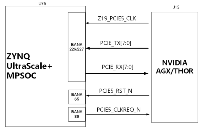
Figure 2.9.1 - MPSoC and ORIN Module Hardware Connection Diagram
PCIe Gen3 x8 and MIPI communication pin assignment is as follows:
| Signal Name | Pin Name | Pin Number | Remarks |
| Z19_PCIE5_CLK_N | 227_CLK0_N | AD11 | PCIe lane reference clock negative |
| Z19_PCIE5_CLK_P | 227_CLK0_P | AD12 | PCIe lane reference clock positive |
| PCIE_RX0_N | 227_TX3_N | AD7 | PCIe lane 0 data receive negative |
| PCIE_RX0_P | 227_TX3_P | AD8 | PCIe lane 0 data receive positive |
| PCIE_RX1_N | 227_TX2_N | AE5 | PCIe lane 1 data receive negative |
| PCIE_RX1_P | 227_TX2_P | AE6 | PCIe lane 1 data receive positive |
| PCIE_RX2_N | 227_TX1_N | AF7 | PCIe lane 2 data receive negative |
| PCIE_RX2_P | 227_TX1_P | AF8 | PCIe lane 2 data receive positive |
| PCIE_RX3_N | 227_TX0_N | AG5 | PCIe lane 3 data receive negative |
| PCIE_RX3_P | 227_TX0_P | AG6 | PCIe lane 3 data receive positive |
| PCIE_RX4_N | 226_TX3_N | AH7 | PCIe lane 4 data receive negative |
| PCIE_RX4_P | 226_TX3_P | AH8 | PCIe lane 4 data receive positive |
| PCIE_RX5_N | 226_TX2_N | AJ5 | PCIe lane 5 data receive negative |
| PCIE_RX5_P | 226_TX2_P | AJ6 | PCIe lane 5 data receive positive |
| PCIE_RX6_N | 226_TX1_N | AK7 | PCIe lane 6 data receive negative |
| PCIE_RX6_P | 226_TX1_P | AK8 | PCIe lane 6 data receive positive |
| PCIE_RX7_N | 226_TX0_N | AL5 | PCIe lane 7 data receive negative |
| PCIE_RX7_P | 226_TX0_P | AL6 | PCIe lane 7 data receive positive |
| PCIE_TX0_N | 227_RX3_N | AE1 | PCIe lane 0 data transmit negative |
| PCIE_TX0_P | 227_RX3_P | AE2 | PCIe lane 0 data transmit positive |
| PCIE_TX1_N | 227_RX2_N | AF3 | PCIe lane 1 data transmit negative |
| PCIE_TX1_P | 227_RX2_P | AF4 | PCIe lane 1 data transmit positive |
| PCIE_TX2_N | 227_RX1_N | AG1 | PCIe lane 2 data transmit negative |
| PCIE_TX2_P | 227_RX1_P | AG2 | PCIe lane 2 data transmit positive |
| PCIE_TX3_N | 227_RX0_N | AH3 | PCIe lane 3 data transmit negative |
| PCIE_TX3_P | 227_RX0_P | AH4 | PCIe lane 3 data transmit positive |
| PCIE_TX4_N | 226_RX3_N | AJ1 | PCIe lane 4 data transmit negative |
| PCIE_TX4_P | 226_RX3_P | AJ2 | PCIe lane 4 data transmit positive |
| PCIE_TX5_N | 226_RX2_N | AK3 | PCIe lane 5 data transmit negative |
| PCIE_TX5_P | 226_RX2_P | AK4 | PCIe lane 5 data transmit positive |
| PCIE_TX6_N | 226_RX1_N | AL1 | PCIe lane 6 data transmit negative |
| PCIE_TX6_P | 226_RX1_P | AL2 | PCIe lane 6 data transmit positive |
| PCIE_TX7_N | 226_RX0_N | AM3 | PCIe lane 7 data transmit negative |
| PCIE_TX7_P | 226_RX0_P | AM4 | PCIe lane 7 data transmit positive |
| PCIE5_CLKREQ_N | B91_L12_P | A10 | PCIe clock request (disable reference clock) |
| PCIE5_RST_N | PCIE_PERSTN | AM25 | PCIe global reset signal |
Table 2.9.1 - PCIe Gen3 x8 Communication Pin Assignment
2.10 LED Indicators and Buttons
The carrier board MPSoC side has 5 user LED indicators and 3 function buttons. Users can programmatically control the on/off state of TEST_LED1, TEST_LED2, and PS_LED (3 LEDs). The 3 function buttons include one user button each for PS and PL sides, plus the SOM power switch button. The hardware connection diagram for LEDs and buttons is shown in Figure 2.10.1:
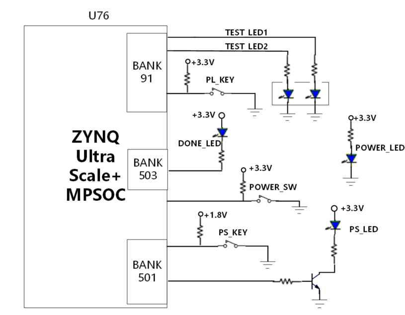
Figure 2.10.1 - User LED Hardware Connection Diagram
The user LED and button pin assignment is shown in the table below:
| Signal Name | Pin Name | Pin Number | Remarks |
| TEST_LED1 | B91_L7_N | E10 | PL-side user LED1 |
| TEST_LED2 | B91_L7_P | E11 | PL-side user LED2 |
| PS_LED | PS_MIO31 | M28 | PS-side user LED |
| PL_KEY | B91_L2_P | H11 | PL-side user test button |
| PS_KEY | PS_MIO43 | R30 | PS-side user test button |
Table 2.10.1 - User LED and Button Pin Assignment
2.11 JTAG Debug Port
The HEA19 development board provides a JTAG interface for downloading ZYNQ UltraScale+ MPSoC programs or programming them into FLASH. To avoid damage to the ZYNQ UltraScale+ MPSoC chip from hot-plugging, protection diodes are added to the JTAG signals to ensure the signal voltage stays within the FPGA's acceptable range.
2.12 DIP Switch Configuration
The development board has a 4-bit DIP switch SW5 for configuring the MPSoC system boot mode. The MPSoC system development platform supports 4 boot modes: JTAG debug mode, QSPI FLASH boot, eMMC boot, and SD 2.0 card boot. After power-up, the MPSoC chip detects the PS_MODE0-3 pin levels to determine the boot mode. Users can select different boot modes via the DIP switch SW5 on the expansion board. The SW5 boot mode configuration is shown in Table 2.12.1.
| SW5 | DIP Switch Position (4,3,2,1) | MODE[3:0] | Boot Mode |
| ON, ON, ON, ON | 0000 | PS JTAG |
| ON, ON, OFF ,ON | 0010 | QSPI FLASH | |
| ON, OFF, ON, OFF | 0101 | SD Card | |
| ON, OFF, OFF, ON | 0110 | EMMC |
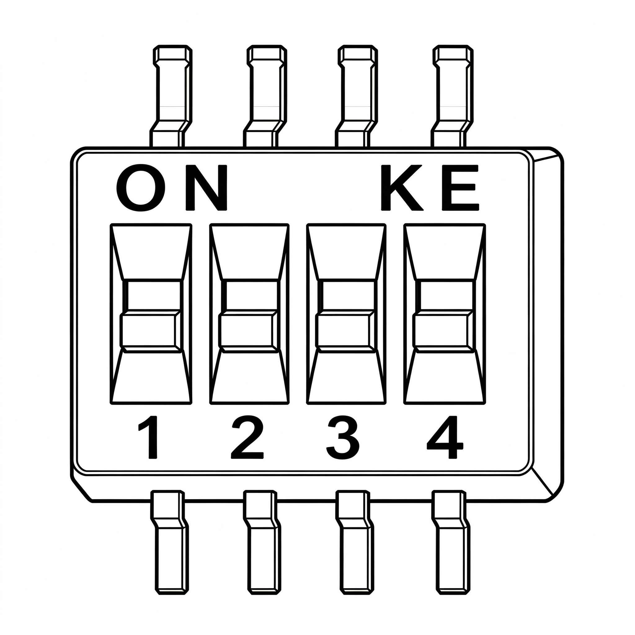
Table 2.12.1 - SW5 Boot Mode Configuration
2.13 Fan
Since the MPSoC generates significant heat during normal operation, a heatsink and fan are added on the board to prevent the chip from overheating. The fan is controlled by the MPSoC chip, with the control pin connected to BANK 91 IO (FPGA pin G11). When the IO output is low, the MOSFET turns on and the fan operates; when the IO output is high, the fan stops. The fan is pre-installed on the development board with screws. The fan power is connected to the J15 connector, with red as positive and black as negative.
Chapter 3 Jetson System
3.1 NVIDIA Jetson Module
The development board features a 699-pin Molex Mirror Mezz connector for connecting either the NVIDIA AGX ORIN module or the AGX THOR module, which users can select according to their needs.
The AGX ORIN module is based on the Ampere GPU, delivering up to 275 TOPS of AI compute, with a 12-core ARM Cortex-A78AE CPU and up to 64GB LPDDR5 memory, suitable for demanding edge AI applications. The AGX THOR module uses a more advanced CPU+GPU+DPU heterogeneous computing architecture, delivering 2000+ INT8 TOPS of AI compute, over 7 times that of the AGX Orin (275 TOPS), and even surpassing some current data center GPU accelerators. It is based on NVIDIA's new-generation GPU architecture and dedicated AI acceleration units, deeply optimized for multimodal large models and Physical AI (enabling machines to understand and simulate the physical world).
The detailed specifications comparison between AGX Orin and THOR T5000 is as follows:
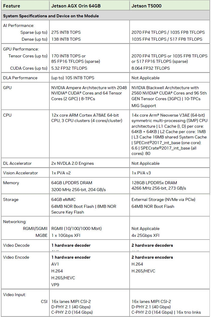
Table 3.1.1 - AGX Orin vs THOR T5000 Specifications Comparison
For detailed information, please refer to the module datasheets "Jetson_AGX_Modules_DS-10662-001_v1.0" and "Jetson_T5000_Modules_DS_DS11945001_v1.1".
3.2 M.2 SSD Interface
The ORIN system has a PCIe (x4) Gen4 standard M.2 interface for connecting NVMe SSD solid-state drives, where ORIN data and system files are stored. The ORIN AGX module uses PCIe x4 (C4) to connect to the M.2 interface, while the ORIN THOR module uses PCIe x2 (C3). The M.2 interface uses an M-key slot, supporting only PCIe (not SATA). Users should select PCIe-type NVMe SSD solid-state drives. The M.2 interface design diagram is shown below:
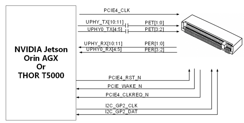
Figure 3.2.1 - M.2 Interface Design Diagram
M.2 SSD interface pin assignment:
| Pin # | Signal Name | Pin Name | Description | Direction |
| D32 | PER3_N | UPHY_RX22_N | UPHY block 0, Receive Lane 4 (Not use for THOR T5000) | Input |
| D33 | PER3_P | UPHY_RX22_P | Input | |
| J34 | PET3_N | UPHY_TX22_N | UPHY block 0, Transmit Lane 4 (Not used for THOR T5000) | Output |
| J35 | PET3_P | UPHY_TX22_P | Output | |
| A35 | PER2_N | UPHY_RX23_N | UPHY block 0, Receive Lane 5 (Not used for THOR T5000) | Input |
| A34 | PER2_P | UPHY_RX23_P | Input | |
| H33 | PET2_N | UPHY_TX23_N | UPHY block 0, Transmit Lane 5 (Not used for THOR T5000) | Output |
| H32 | PET2_P | UPHY_TX23_P | Output | |
| B13 | PER1_N | UPHY_RX10_N | UPHY block 0, Receive Lane 6 | Input |
| B12 | PER1_P | UPHY_RX10_P | Input | |
| K12 | PET1_N | UPHY_TX10_N | UPHY block 0, Transmit Lane 6 | Output |
| K13 | PET1_P | UPHY_TX10_P | Output | |
| D13 | PER0_N | UPHY_RX11_N | UPHY block 0, Receive Lane 7 | Input |
| D12 | PER0_P | UPHY_RX11_P | Input | |
| H13 | PET0_N | UPHY_TX11_N | UPHY block 0, Transmit Lane 7 | Output |
| H12 | PET0_P | UPHY_TX11_P | Output | |
| E22 | PCIE4_CLK_N | PEX_CLK4_N | AGX:PCIe output Reference Clock for controller #4. THOR:PCIe output Reference Clock for controller #3. | Output |
| E23 | PCIE4_CLK_P | PEX_CLK4_P | Output | |
| G8 | PEX_C4_CLKREQ_N | GP183_PCIE4_ CLKREQ_N | AGX:PCIe Clock Request for controller #4. THOR:PCIe Clock Request for controller #3. | Input |
| J9 | PEX_C4_RST_N | GP184_PCIE4_RST_N | AGX:PCIe Reset for controller #4. THOR:PCIe Reset for controller #3. | Output |
| A8 | PCIE_WAKE_N | PEX_WAKE_N | PCIe Wake. | Input |
Table 3.2.1 - M.2 SSD Interface Pin Assignment
3.3 M.2 WiFi/BT Interface
The HEA19 development board has an M.2 KEY E connector reserved for WiFi/BT modules. The interface includes PCIe x1, USB2.0, UART, I2S, and I2C signals.
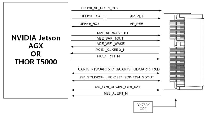
Figure 3.3.1 - M.2 Connection Diagram
M.2 WiFi/BT interface pin assignment:
| Pin # | Signal Name | Pin Name | Description | Direction |
| B32 | AP_PERN0 | UPHY_RX21_N | UPHY block 0, Receive Lane 3 | Input |
| B33 | AP_PERP0 | UPHY_RX21_P | Input | |
| G34 | AP_PETN0 | UPHY_TX21_N | UPHY block 0, Transmit Lane 3 | Output |
| G35 | AP_PETP0 | UPHY_TX21_P | Output | |
| D48 | UPHY0_SF_PCIE1_CLK_N | PEX_CLK6_N | PCIe Output Reference Clock for controller #1. | Output |
| D49 | UPHY0_SF_PCIE1_CLK_P | PEX_CLK6_P | Output | |
| B37 | PCIE1_CLKREQ_N | PEX_C7_CLKREQ_N | PCIe Clock Request for controller #1. | Input |
| A57 | M2E_AP_WAKE_BT | UART2_CTS | BT and AP wake up signal | Input |
| G58 | M2E_SAR_TOUT | UART2_RTS | Reserve | Output |
| G55 | M2E_WIFI_WAKE | GPIO23 | WIFI Wake signal | Input |
| J58 | UART5_TXD | UART5_TX | UART 5 Transmit | Output |
| H58 | UART5_RXD | UART5_RX | UART 5 Receive | Input |
| K58 | UART5_RTS | UART5_RTS | UART 5 Request to Send | Output |
| H57 | UART5_CTS | UART5_CTS | UART 5 Clear to Send | Input |
| C59 | I2S4_SCLK | I2S3_SCLK | I2S Serial Clock | Output |
| C60 | I2S4_FS | I2S3_FS | I2S Left/Right Clock | Output |
| J59 | I2S4_DIN | I2S3_DIN | I2S Data Input | Input |
| K59 | I2S4_DOUT | I2S3_DOUT | I2S Data Output | Output |
Table 3.3.1 - M.2 WiFi/BT Interface Pin Assignment
3.4 DP Display Interface
The Jetson Orin AGX/THOR module supports DP video output. The development board has 1x DisplayPort output interface connected to the Jetson Orin AGX/THOR module for video display. The interface supports VESA DisplayPort V1.2 and eDP V1.4 output standards.
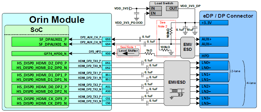
DisplayPort interface pin assignment is as follows:
| Pin # | Signal Name | Pin Name | Description | Direction |
| D52 | HDMI_DP2_TX0_N | HS_DISP0_HDMI_D2_DP0_N | DisplayPort 2 Lane 0- | Output |
| D51 | HDMI_DP2_TX0_P | HS_DISP0_HDMI_D2_DP0_P | DisplayPort 2 Lane 0+ | Output |
| B52 | HDMI_DP2_TX1_N | HS_DISP0_HDMI_D1_DP1_N | DisplayPort 2 Lane 1– | Output |
| B51 | HDMI_DP2_TX1_P | HS_DISP0_HDMI_D1_DP1_P | DisplayPort 2 Lane 1+ | Output |
| A50 | HDMI_DP2_TX2_N | HS_DISP0_HDMI_D0_DP2_N | DisplayPort 2 Lane 2– | Output |
| A51 | HDMI_DP2_TX2_P | HS_DISP0_HDMI_D0_DP2_P | DisplayPort 2 Lane 2+ | Output |
| C50 | HDMI_DP2_TX3_N | HS_DISP0_HDMI_CK_DP3_N | DisplayPort 2 Lane 3– | Output |
| C51 | HDMI_DP2_TX3_P | HS_DISP0_HDMI_CK_DP3_P | DisplayPort 2 Lane 3+ | Output |
| K50 | DP2_HPD | GP74_HPD0_N | Display Port/HDMI 2 Hot Plug Detect | Bidir |
| J50 | HDMI_CEC | GP05_HDMI_CEC | HDMI CEC | Bidir |
| G53 | DP2_AUX_CH_P | SF_DPAUX01_P | Display Port 2 Aux+ or HDMI DDC SCL | Bidir |
| G54 | DP2_AUX_CH_N | SF_DPAUX01_N | Display Port 2 Aux– or HDMI DDC SDA | Bidir |
Table 3.4.1 - DisplayPort Interface Pin Assignment
3.5 USB3.2 Interface
The 2x USB3.2 interfaces (USB0 and USB1) of the NVIDIA Orin AGX/THOR module are connected to USB3.2 Type-C connectors. The USB interfaces support HOST, SLAVE, and OTG modes, with a data transfer rate up to 10Gb/s. The USB3.2 connection diagram is shown in Figure 3.5.1:
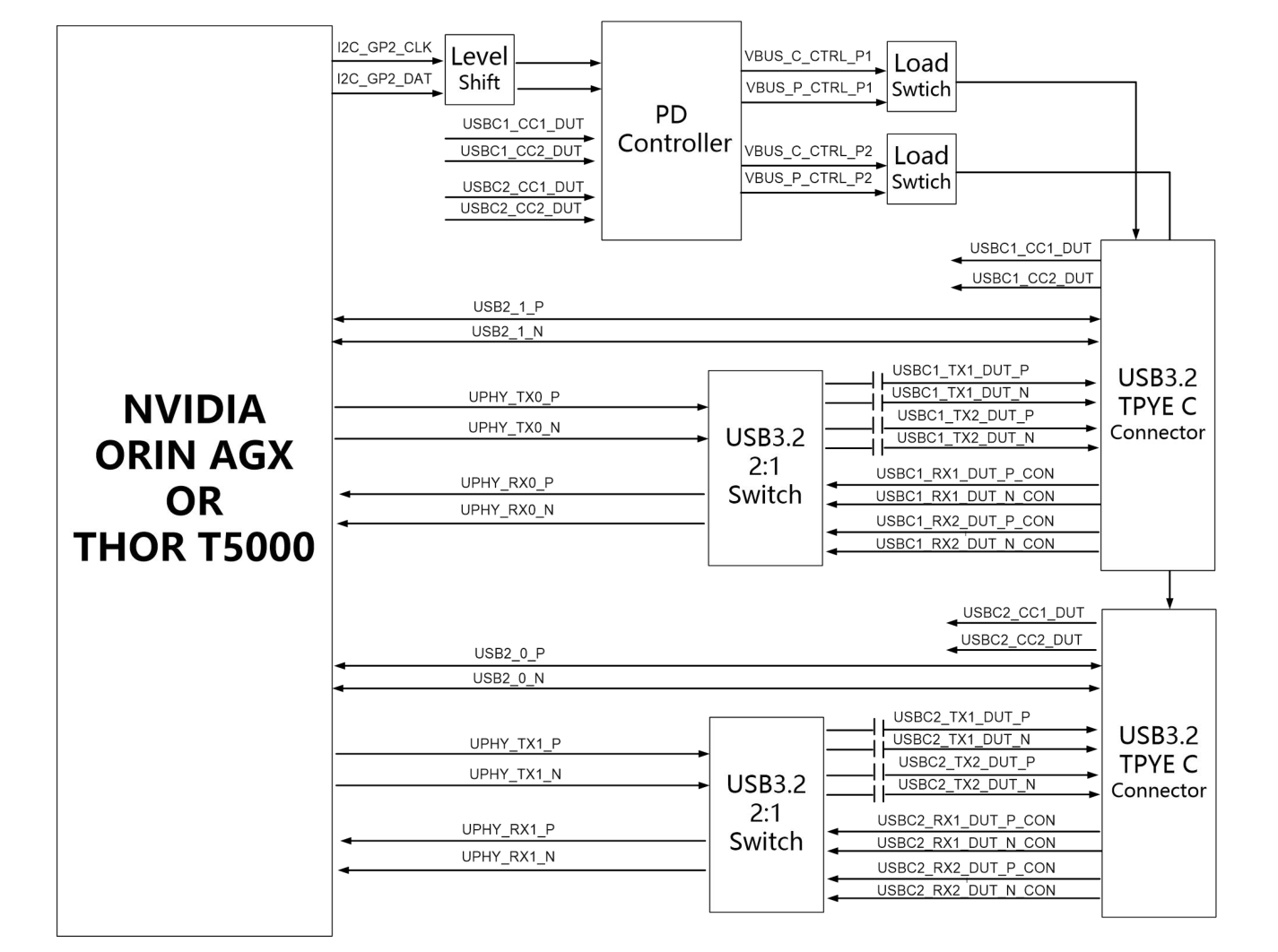
Figure 3.5.1 - USB3.2 Interface Diagram
USB3.2 interface pin assignment:
| Pin # | Signal Name | Pin Name | Description | Direction |
| A23 | UPHY_RX0_N | HS_UPHY0_L0_RX_N | UPHY block 0, Receive Lane 0 | Input |
| A22 | UPHY_RX0_P | HS_UPHY0_L0_RX_P | Input | |
| J23 | UPHY_TX0_N | HS_UPHY0_L0_TX_N | UPHY block 0, Transmit Lane 0 | Output |
| J22 | UPHY_TX0_P | HS_UPHY0_L0_TX_P | Output | |
| F13 | USB0_N | HS_USB0_P0_N | USB 2.0 Port 0 Data | Bidir |
| F12 | USB0_P | HS_USB0_P0_P | Bidir | |
| C22 | UPHY_RX1_N | HS_UPHY0_L1_RX_N | UPHY block 0, Receive Lane 1 | Input |
| C23 | UPHY_RX1_P | HS_UPHY0_L1_RX_P | Input | |
| G22 | UPHY_TX1_N | HS_UPHY0_L1_TX_N | UPHY block 0, Transmit Lane 1 | Output |
| G23 | UPHY_TX1_P | HS_UPHY0_L1_TX_P | Output | |
| C10 | USB1_N | HS_USB2_P1_N | USB 2.0, Port 1 Data | Bidir |
| C11 | USB1_P | HS_USB2_P1_P | Bidir | |
| J61 | I2C_GP2_CLK | I2C2_CLK | General I2C 2 clock | Bidir |
| K61 | I2C_GP2_DAT | I2C2_DAT | General I2C 2 Data | Bidir |
| E56 | I2C_INT_CCG4 | SPI3_CS1_N | General I2C interrupt | Input |
Table 3.5.1 - USB3.2 Pin Configuration
3.6 10G Ethernet Interface (AGX only)
When using the AGX ORIN module, the expansion board provides 1x 10G Ethernet interface. The AGX ORIN module's Multi-Gigabit Ethernet (MGBE) is connected to a Marvell 10Gbps Ethernet PHY chip. The AQR113C is a quad-channel 10GBASE-T Ethernet PHY chip that supports 10Gbps Ethernet transmission over twisted pair (Cat6a/Cat7 cables), with backward compatibility for 5Gbps, 2.5Gbps, 1Gbps, and 100Mbps. The MDI signals output from the AQR113C are directly connected to the RJ45 connector. Figure 3.6.1 shows the Ethernet connection diagram:
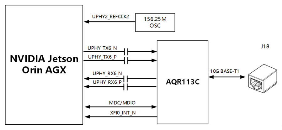
Figure 3.6.1 - Ethernet Connection Diagram
NVIDIA Jetson Orin AGX 10G Ethernet pin assignment is as follows:
| Pin # | Signal Name | Pin Name | Description | Direction |
| K16 | UPHY_TX6_N | HS_UPHY2_L4_TX_N | UPHY block 2, Transmit Lane 4 | Output |
| K17 | UPHY_TX6_P | HS_UPHY2_L4_TX_P | Output | |
| B17 | UPHY_RX6_N | HS_UPHY2_L4_RX_N | UPHY block 2, Receive Lane 4 | Input |
| B16 | UPHY_RX6_P | HS_UPHY2_L4_RX_P | Input | |
| H51 | GPIO26_XFI0_MDC | GPIO26 | MGBE C0 Management Clock | Bidir |
| K49 | GPIO25_XFI0_MDIO | GPIO25 | MGBE C0 Management Data | Bidir |
| C57 | XFI0_INT_N | SPI3_CS0_N | MGBE C0 interrupt signal | Input |
| F29 | UPHY_REFCLK2_N | HS_UPHY2_REFCLK2_N | This is the REFCLK for MGBE. | Input |
| F28 | UPHY_REFCLK2_P | HS_UPHY2_REFCLK2_P | Input |
Table 3.6.1 - NVIDIA Jetson Orin AGX 10G Ethernet Pin Assignment
3.7 5G Ethernet Interface (THOR only)
When using the THOR T5000 module, the expansion board provides 1x 5Gbps Ethernet interface. The THOR T5000 module achieves 5G Gigabit communication via a PCIe network controller (NIC). The 5G Ethernet chip uses Realtek RTL8126. The RTL8126 is a quad-channel 10GBASE-T Ethernet PHY chip that supports 10Gbps Ethernet transmission over twisted pair (Cat6a/Cat7 cables), with backward compatibility for 5Gbps, 2.5Gbps, 1Gbps, and 100Mbps. The MDI signals output from the RTL8126 are directly connected to the RJ45 connector. Figure 3.7.1 shows the Ethernet connection diagram:
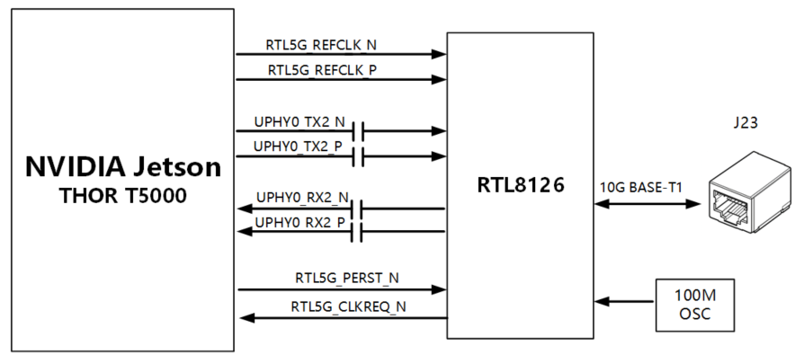
Figure 3.7.1 - Ethernet Connection Diagram
NVIDIA Jetson THOR T5000 5G Ethernet pin assignment is as follows:
| Pin # | Signal Name | Pin Name | Description | Direction |
| E15 | RTL5G_REFCLK_P | UPHY_REFCLK5_P | PCIe output Reference Clock for controller #2 | Output |
| E14 | RTL5G_REFCLK_N | UPHY_REFCLK5_N | Output | |
| B21 | UPHY_RX2_P | UPHY_RX2_P | Differential Receive Data Pair | Input |
| B20 | UPHY_RX2_N | UPHY_RX2_N | Input | |
| K21 | UPHY_TX2_P | UPHY_TX2_P | Differential Transmit Data Pair | Output |
| K20 | UPHY_TX2_N | UPHY_TX2_N | Output | |
| D10 | RTL5G_PERST_N | PEX_C2_RST_N | PCIe Reset for controller #2 | Output |
| E11 | RTL5G_CLKREQ_N | PEX_C2_CLKREQ_N | PCIe Clock Request for controller #2 | Input |
Table 3.7.1 - NVIDIA Jetson THOR T5000 5G Ethernet Pin Assignment
3.8 TF Card (AGX only)
The HEA19 board has a TF card slot on the ORIN AGX system side. The AGX SDMMC controller is directly connected to the TF card via the SDIO interface. The schematic of the AGX module and TF card connector is shown below.
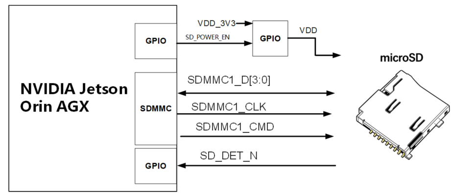
Figure 3.8.1 - TF Card Connection Diagram
NVIDIA Jetson Orin AGX TF card pin assignment is as follows:
| Pin # | Signal Name | Pin Name | Description | Direction |
| B6 | SDMMC1_CLK | SDCARD_CLK | SD Card (or SDIO) Clock | Output |
| A5 | SDMMC1_CMD | SDCARD_CMD | SD Card (or SDIO) Command | Bidir |
| E8 | SDMMC1_D0 | SDCARD_D0 | SD Card (or SDIO) Data 0 | Bidir |
| F8 | SDMMC1_D1 | SDCARD_D1 | SD Card (or SDIO) Data 1 | Bidir |
| A4 | SDMMC1_D2 | SDCARD_D2 | SD Card (or SDIO) Data 2 | Bidir |
| D6 | SDMMC1_D3 | SDCARD_D3 | SD Card (or SDIO) Data 3 | Bidir |
| L6 | SD_DET_N | GPIO02 | GPIO #2 pr SD Card Card Detect | Bidir |
| A7 | SD_POWER_EN | GPIO29 | GPIO #29, I2S, or SD Card Write Protect | Bidir |
Table 3.8.1 - NVIDIA Jetson Orin AGX TF Card Pin Assignment
3.9 PCIe x8 Interface
The ORIN AGX/THOR system and MPSoC are connected via PCIe Gen3 x8 for PCIe data communication. In PCIe communication, the NVIDIA AGX/THOR is the default RC master device, and the MPSoC is the EP slave device. Figure 3.9.1 shows the PCIe hardware connection diagram between the AGX/THOR module and MPSoC.
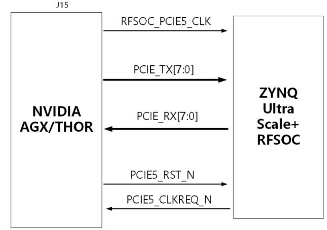
Figure 3.9.1 - PCIe Gen3 x8 Connection Diagram
NVIDIA Jetson Orin AGX/THOR PCIe x8 pin assignment is as follows:
| Pin # | Signal Name | Pin Name | Description | Direction |
| D25 | PCIE_RX0_N | UPHY_RX12_N | UPHY block 1, Receive Lane 0 | Input |
| D24 | PCIE_RX0_P | UPHY_RX12_P | Input | |
| B24 | PCIE_RX1_N | UPHY_RX13_N | UPHY block 1, Receive Lane 1 | Input |
| B25 | PCIE_RX1_P | UPHY_RX13_P | Input | |
| C26 | PCIE_RX2_N | UPHY_RX14_N | UPHY block 1, Receive Lane 2 | Input |
| C27 | PCIE_RX2_P | UPHY_RX14_P | Input | |
| A27 | PCIE_RX3_N | UPHY_RX15_N | UPHY block 1, Receive Lane 3 | Input |
| A26 | PCIE_RX3_P | UPHY_RX15_P | Input | |
| D29 | PCIE_RX4_N | UPHY_RX16_N | UPHY block 1, Receive Lane 4 | Input |
| D28 | PCIE_RX4_P | UPHY_RX16_P | Input | |
| B28 | PCIE_RX5_N | UPHY_RX17_N | UPHY block 1, Receive Lane 5 | Input |
| B29 | PCIE_RX5_P | UPHY_RX17_P | Input | |
| C30 | PCIE_RX6_N | UPHY_RX18_N | UPHY block 1, Receive Lane 6 | Input |
| C31 | PCIE_RX6_P | UPHY_RX18_P | Input | |
| A31 | PCIE_RX7_N | UPHY_RX19_N | UPHY block 1, Receive Lane 7 | Input |
| A30 | PCIE_RX7_P | UPHY_RX19_P | Input | |
| H25 | PCIE_TX0_N | UPHY_TX12_N | UPHY block 1, Transmit Lane 0 | Output |
| H24 | PCIE_TX0_P | UPHY_TX12_P | Output | |
| K24 | PCIE_TX1_N | UPHY_TX13_N | UPHY block 1, Transmit Lane 1 | Output |
| K25 | PCIE_TX1_P | UPHY_TX13_P | Output | |
| G26 | PCIE_TX2_N | UPHY_TX14_N | UPHY block 1, Transmit Lane 2 | Output |
| G27 | PCIE_TX2_P | UPHY_TX14_P | Output | |
| J27 | PCIE_TX3_N | UPHY_TX15_N | UPHY block 1, Transmit Lane 3 | Output |
| J26 | PCIE_TX3_P | UPHY_TX15_P | Output | |
| H29 | PCIE_TX4_N | UPHY_TX16_N | UPHY block 1, Transmit Lane 4 | Output |
| H28 | PCIE_TX4_P | UPHY_TX16_P | Output | |
| K28 | PCIE_TX5_N | UPHY_TX17_N | UPHY block 1, Transmit Lane 5 | Output |
| K29 | PCIE_TX5_P | UPHY_TX17_P | Output | |
| G30 | PCIE_TX6_N | UPHY_TX18_N | UPHY block 1, Transmit Lane 6 | Output |
| G31 | PCIE_TX6_P | UPHY_TX18_P | Output | |
| J31 | PCIE_TX7_N | UPHY_TX19_N | UPHY block 1, Transmit Lane 7 | Output |
| J30 | PCIE_TX7_P | UPHY_TX19_P | Output | |
| C8 | PCIE5_CLKREQ_N | PEX_C5_CLKREQ_N | PCIe Clock Request for controller #5 | Input |
| H10 | PCIE5_RST_N | PEX_C5_RST_N | PCIe Reset for controller #5 | Output |
Table 3.9.1 - NVIDIA AGX/THOR PCIe x8 Pin Assignment
3.10 EEPROM
The HEA19 board has an EEPROM chip on the ORIN AGX/THOR system side, used to store board ID information or configuration data. The chip model is 24AA04 I/SN with 4Kbit capacity, connected to the NVIDIA Jetson AGX/THOR module via the IIC bus. The pin assignment for EEPROM communication with the AGX/THOR module is as follows:
| Pin # | Signal Name | Pin Name | Description | Direction |
| K5 | I2C1_CLK | GP126_I2C1_CLK | I2C1_CLK | Output |
| L8 | I2C1_DAT | GP127_I2C1_DAT | I2C1_DAT | Bidir |
Table 3.10.1 - EEPROM to NVIDIA AGX/THOR Module Communication Pin Assignment
3.11 UART Interface
The HEA19 board provides a UART-to-USB interface on the ORIN AGX/THOR system side. The conversion chip uses Silicon Labs CP2102 USB-UART chip, with a Type-C USB connector. It can be connected to a PC USB port via a USB cable for serial data communication, used for ORIN AGX/THOR program debugging. The USB UART circuit design diagram is shown below.
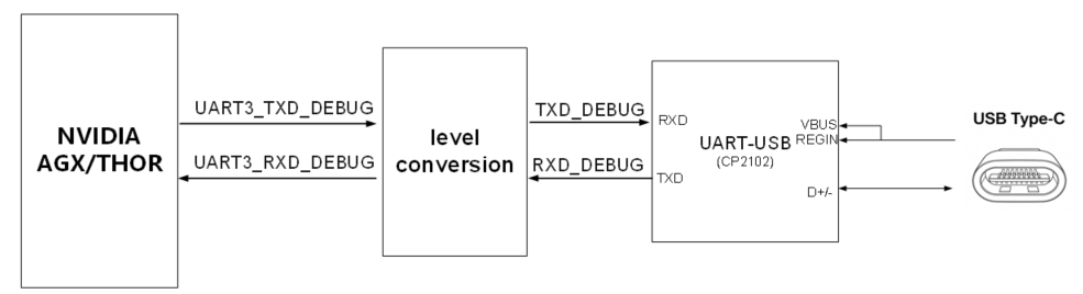
Figure 3.11.1 - Serial to USB Diagram
AGX/THOR module serial-to-USB pin assignment:
| Pin # | Signal Name | Pin Name | Description | Direction |
| H62 | UART3_TX_DEBUG | GP11_UART3_TXD | Debug UART Transmit | Output |
| K60 | UART3_RX_DEBUG | GP12_UART3_RXD | Debug UART Receive | Input |
Table 3.11.1 - Serial to USB Pin Assignment
3.12 40-Pin Connector
The HEA19 board has a 40-pin connector on the ORIN AGX/THOR system side for expanding AGX/THOR GPIO or peripheral interfaces. The 40-pin connector expands 2x I2C, 2x SPI, 1x UART, 2x CAN, 1x I2S, 2x PWM signals, and several GPIOs. All signals are connected to the AGX/THOR module through bidirectional level shifter chips. The default IO level on the connector is 3.3V. The pin assignment for the 40-pin connector to AGX/THOR module communication is as follows:
| 40-Pin # | Signal Name | Description | 40-Pin # | Signal Name | Description |
| 1 | VDD_3V3 | +3.3V Power | 2 | VDD_5V | +5V Power |
| 3 | I2C_GP8_DAT_LVS | I2C GP8 Data | 4 | VDD_5V | +5V Power |
| 5 | I2C_GP8_CLK_LVS | I2C GP8 Clock | 6 | GND | Ground |
| 7 | MCLK05_LVS | MCLK05 | 8 | UART1_TX_LVS | UART1 TXD transmit |
| 9 | GND | Ground | 10 | UART1_RX_LVS | UART1 RXD receive |
| 11 | UART1_RTS_LVS | UART1 RTS | 12 | I2S2_SCLK_LVS | I2S2 SCLK clock |
| 13 | PWM1_40PIN_LVS | PWM1 control signal | 14 | GND | Ground |
| 15 | PWM2_40PIN_LVS | PWM2 control signal | 16 | GPIO8_DMIC3_DAT_40PIN | GPIO8 |
| 17 | VDD_3V3 | +3.3V Power | 18 | PWM3_40PIN_LVS | PWM3 control signal |
| 19 | SPI_MOSI_LVS | SPI MOSI | 20 | GND | Ground |
| 21 | SPI_MISO_LVS | SPI MISO | 22 | GPIO_40PIN_LVS | GPIO signal |
| 23 | SPI_SCK_LVS | SPI SCK clock signal | 24 | SPI_CS0_LVS | SPI CS0 chip select |
| 25 | GND | Ground | 26 | SPI_CS1_LVS | SPI CS1 chip select |
| 27 | I2C_GP2_DAT_LVS | I2C GP2 Data | 28 | I2C_GP2_CLK_LVS | I2C GP2 Clock |
| 29 | CAN0_DIN | CAN0 Data Input | 30 | GND | Ground |
| 31 | CAN0_DOUT | CAN0 Data Output | 32 | GPIO9_DMIC3_CLK_40PIN | GPIO9 |
| 33 | CAN1_DOUT | CAN1 Data Output | 34 | GND | Ground |
| 35 | I2S2_FS_LVS | I2S2 FS frame sync | 36 | UART1_CTS_LVS | UART1 CTS |
| 37 | CAN1_DIN | CAN1 Data Input | 38 | I2S2_DIN_LVS | I2S2 Data Input |
| 39 | GND | Ground | 40 | I2S2_DOUT_LVS | I2S2 Data output |
Table 3.12.1 - 40-Pin Header Pin Assignment
Chapter 4 Power Supply
The HEA19 development board is powered by +12V (25A). The 12V power supply directly powers the MPSoC SOM through a MOSFET switch, controlled by the VIN_POW_ON signal output from the MCU. The 12V and 5V power supplies for the AGX/THOR module are also controlled and output via VIN_POW_ON.
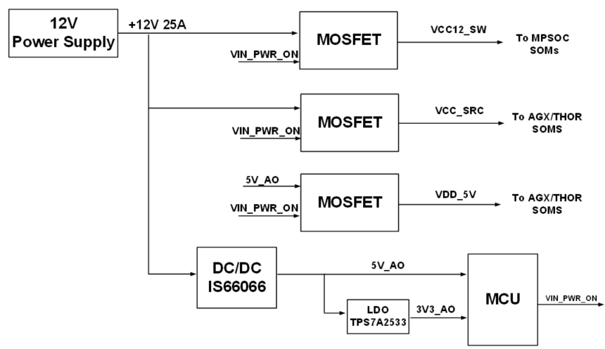
Figure 4.1.1 - 12V and 5V Power Supply Design Diagram
The HEA19 carrier board MCU chip controls the power-up sequencing of the entire board. This design is consistent with the AGX/THOR Demo board. The MCU circuit design is as follows:
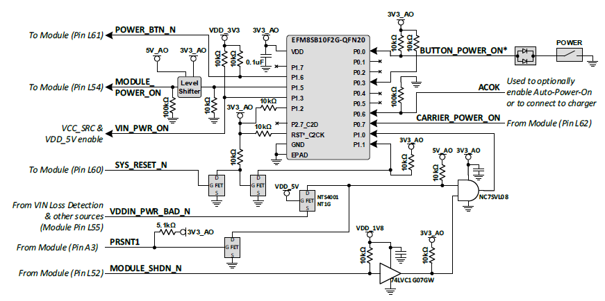
Figure 4.1.2 - MCU Control Block Diagram
- Power-On
When the POWER button is pressed, the MCU controls VIN_PWR_ON to output a high level, and the AGX/THOR module begins to be powered. Then the MODULE_POWER_ON signal outputs a high level to notify the AGX/THOR module to start. After the AGX/THOR module finishes booting, it outputs a high CARRIER_POWER_ON signal. The CARRIER_POWER_ON signal enables the 3.3V, 1.8V, and other power rails on the board, and the peripherals begin to power up.
- Power-Off
When the POWER button is pressed for more than 10 seconds, the MCU outputs a low MODULE_POWER_ON signal, and the AGX/THOR module begins to power down. At the same time, the AGX/THOR module outputs a low CARRIER_POWER_ON signal, and the peripheral circuits power off. Then the MCU outputs a low VIN_PWR_ON signal.
The detailed HEA19 power sequencing is as follows:
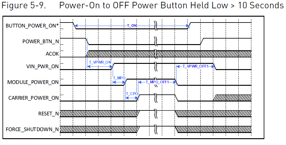
Figure 4.1.3 - Power Sequencing Diagram
Chapter 5 Power Button
The HEA19 development board has 1 power switch button, which is a self-resetting button with an LED indicator. The button signal BUTTON_POWER_ON_N is connected to the MCU P0.0 pin. Users can use this switch button to control board power-on and power-off.
To power on, press the power switch once to start the power supply. To power off, press and hold the power switch (10+ seconds) to turn off the power. If the AGX/THOR module is not installed and the user needs to debug the MPSoC functionality standalone, install the jumper on J17 to pull the MCU P0.3 pin low, and the MCU will power on the board independently. If the AGX/THOR module is installed, the J17 jumper does not need to be installed.
Chapter 6 Mechanical Dimensions
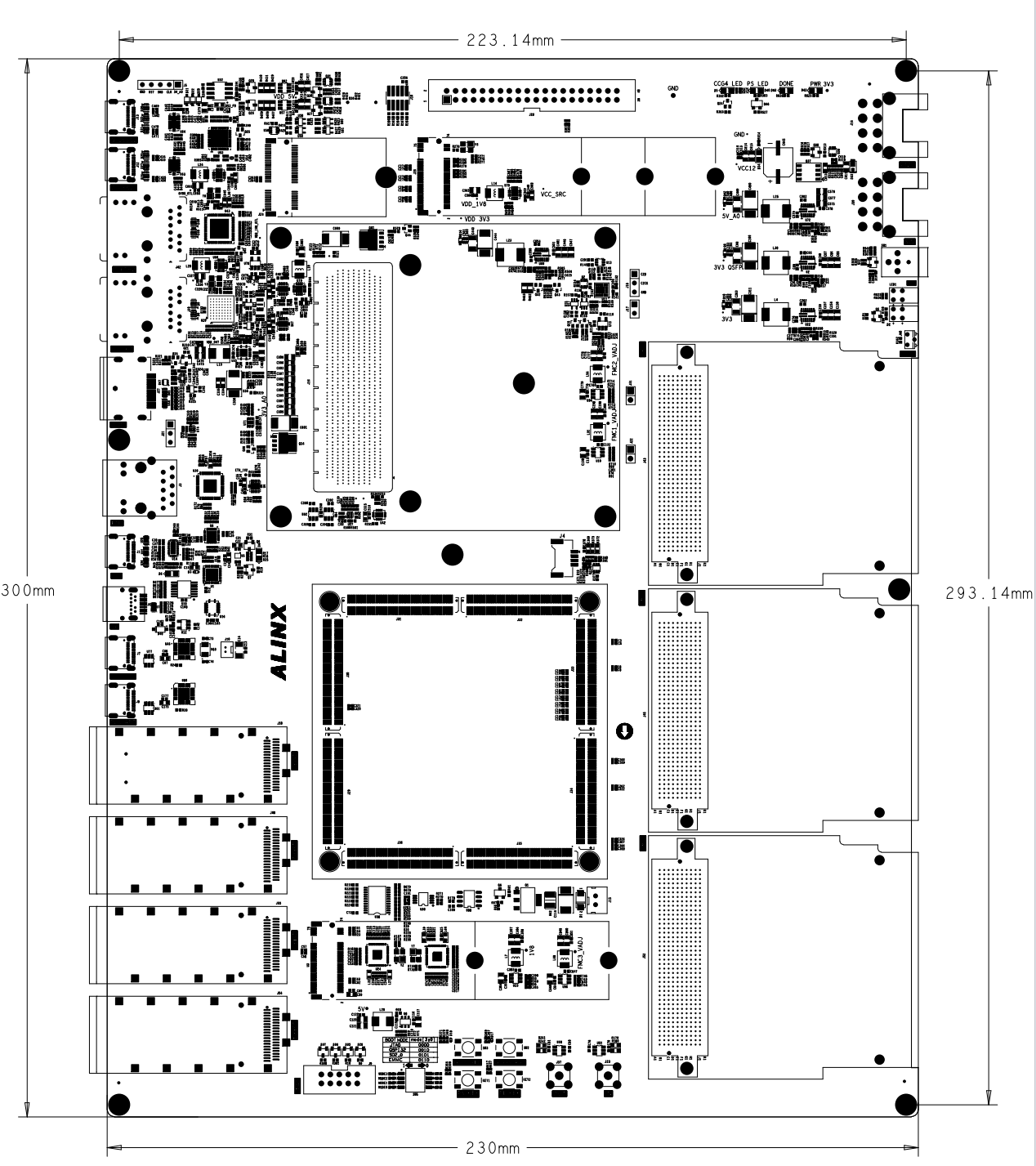
Figure 6.1.1 - Top View
Appendix: List of Abbreviations
| Abbreviation | Full English Name | Description |
| PS | Processor System | The processing subsystem in an SoC, typically including CPU cores, memory controllers, and peripheral interfaces for running software and operating systems. |
| PL | Programmable Logic | User-configurable FPGA logic resources used to implement custom digital circuits, interface controllers, and hardware acceleration functions. |
| SOC | System on Chip | An integrated circuit that combines processors, memory controllers, peripheral interfaces, and other system functions on a single chip. |
| DDR3 | Double Data Rate 3 SDRAM | A third-generation synchronous dynamic memory technology that transfers data on both edges of the clock signal and is commonly used as system memory. |
| eMMC | Embedded Multi Media Card | An embedded non-volatile storage device that integrates NAND Flash memory and a storage controller in a single package. |
| QSPI | Quad Serial Peripheral Interface | A high-speed serial interface that uses four data lines and is commonly used to connect NOR Flash devices for boot or configuration storage. |
| GTP | Gigabit Transceiver | A high-speed serial transceiver integrated in an FPGA for transmitting and receiving data at multi-gigabit rates. |
| UART | Universal Asynchronous Receiver/Transmitter | An asynchronous serial communication interface that transmits and receives data through TX and RX signal lines. |
| HDMI | High-Definition Multimedia Interface | A digital multimedia interface used to transmit high-definition video and audio signals between source and display devices. |
| PCIe | Peripheral Component Interconnect Express | A high-speed serial expansion bus standard used for communication between processors and devices such as FPGAs, GPUs, and SSDs. |
| USB | Universal Serial Bus | A standard serial interface used for data communication, peripheral connection, and power delivery between electronic devices. |
| JTAG | Joint Test Action Group | A standardized interface used for device testing, boundary scan, FPGA programming, and processor or system debugging. |
| SFP | Small Form-factor Pluggable | A compact, hot-pluggable transceiver interface used for optical or electrical network communication. |
| MIO | Multiplexed I/O | Multiplexed processor I/O pins in an SoC that can be configured for functions such as UART, I2C, SPI, or GPIO. |
| GPHY | Gigabit Ethernet PHY | A Gigabit Ethernet physical-layer transceiver that converts digital Ethernet data into electrical signals for transmission over a physical network medium. |
| I2C | Inter-Integrated Circuit | A two-wire serial communication bus using SDA and SCL lines, commonly used to connect sensors, EEPROMs, and peripheral devices. |
| RGMII | Reduced Gigabit Media Independent Interface | A reduced-pin-count interface between an Ethernet MAC and PHY that supports 10, 100, and 1000 Mbps Ethernet communication. |
| RMII | Reduced Media Independent Interface | A reduced-pin-count interface between an Ethernet MAC and PHY, mainly used for 10 and 100 Mbps Ethernet communication. |
| LED | Light Emitting Diode | A semiconductor device that emits light when electrically driven and is commonly used for power, status, and fault indication. |
| LVDS | Low-Voltage Differential Signaling | A high-speed differential signaling standard that provides low power consumption, low noise, and strong resistance to electromagnetic interference. |
Contact information
Alinx Electronic Limited
Company Website: www.en.alinx.com
Service Hotline: +86 21 67676997
Technical Support:technical@alinx.com