
Appearance
PI-ZN010-F1-1 User Manual

Alinx Electronic Limited
Company Website: www.en.alinx.com
Service Hotline: +86 21 67676997
Technical Support : technical@alinx.com
Document Information
| Item | Content |
| Document Name | User Manual |
| Product Model | PI-ZN010-F1-1 |
| Document Version | V1.0 |
| Prepared by | Alinx Electronic Limited |
| Release Date | 2026.10.13 |
Document Revision History
| Version | Date | Section | Revision Summary |
| V1.0 | 2026.10.13 | All | Initial Release |
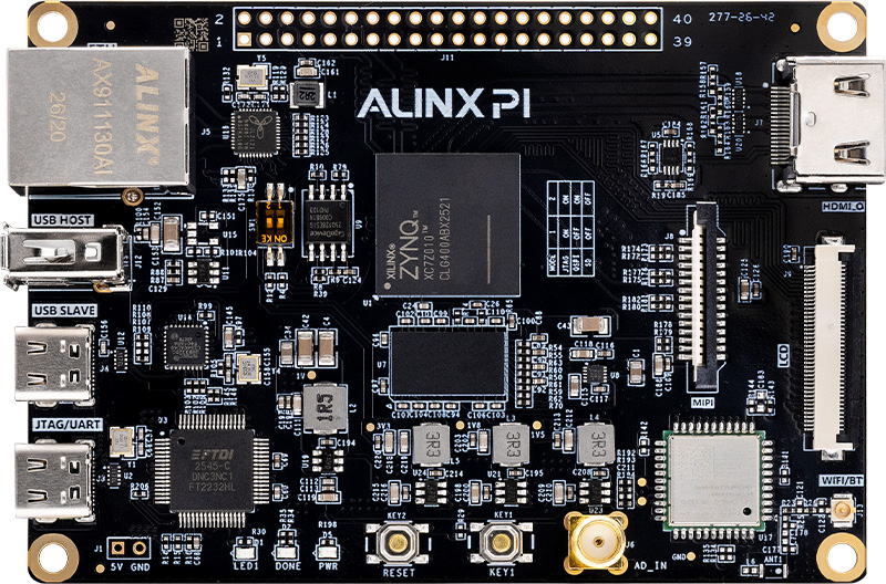
The development board based on the XILINX ZYNQ7000 development platform, model PI-ZN010-F1-1, was officially released in 2026. This development platform is a solution built on Xilinx's Zynq-7000 SoC chips. It uses ARM+FPGA SoC technology to integrate a dual-core ARM Cortex-A9 and FPGA programmable logic into a single chip. It uses the Xilinx Zynq-7000 series XC7Z010-1CLG400C as the core processor, offering rich hardware resources and peripheral interfaces on both the ARM and FPGA sides. The design adheres to the philosophy of "exquisite, practical and concise." It is suitable not only for software engineers to conduct early-stage software verification, but also for hardware engineers to carry out hardware design and software/hardware system co-development, accelerating the project development process.
Chapter 1 Introduction
Here we provide a brief introduction to the features of this ZYNQ7000 development platform, the PI-ZN010-F1-1.
This development board uses a Xilinx Zynq-7000 series chip, model XC7Z010-1CLG400C, in a 400-pin FBGA package. The ZYNQ7000 chip can be divided into the Processor System (PS) and the Programmable Logic (PL). On the PI-ZN010-F1-1 development board, both the PS and the PL of the ZYNQ7000 are equipped with rich external interfaces and devices for convenient use and functional verification. In addition, the board integrates a Xilinx USB Cable downloader circuit, so users only need a USB cable to download and debug the board. Figure 1.1.1 shows the system block diagram of the PI-ZN010-F1-1:
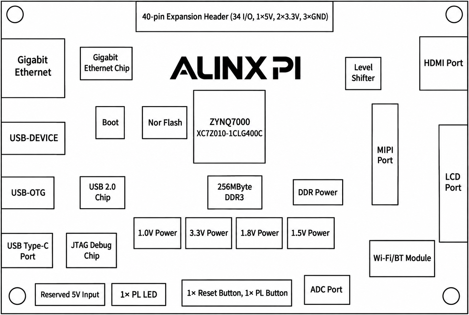
Figure 1.1.1 – PI-ZN010-F1-1 System Block Diagram
From this block diagram, we can see the interfaces and functions of this development platform:
TYPE-C power input, with a reserved external 5V power connector;
Xilinx ARM+FPGA chip Zynq-7000 XC7Z010-1CLG400C;
One 2Gbit high-speed DDR3 SDRAM, which can be used as data cache for the ZYNQ chip or as memory for running an operating system;
One 128Mbit QSPI FLASH, used for storing the ZYNQ chip's system files and user data;
One 10/100/1000M Ethernet RJ-45 interface for Ethernet data exchange with a PC or other network devices;
One HDMI video output interface, supporting 1080P video transmission;
One LCD interface, compatible with a 4.3-inch TFT module;
One MIPI camera interface, compatible with the Alinx MIPI OV5640 camera;
One high-speed USB2.0 HOST/DEVICE interface for connecting USB peripherals such as a mouse, keyboard and USB flash drive to the board;
One high-speed USB2.0 OTG interface for OTG communication with a PC or USB devices;
1 PL-controlled LED;
2 buttons: 1 CPU reset button and 1 PL-controlled button;
An onboard 33.333MHz active crystal oscillator providing a stable clock source for the PS system, and a 50MHz active crystal oscillator providing an additional clock for the PL logic;
One 40-pin expansion connector (2.54mm pitch) for expanding the IO of the ZYNQ PL, compatible with expansion modules such as 7-inch TFT modules, camera modules and AD/DA modules;
One TYPE-C interface for debugging and downloading the ZYNQ system via a TYPE-C cable and the onboard JTAG circuit;
1 Micro SD card slot (on the back of the board) for storing the operating system image and file system.
Chapter 2 Structure and Dimensions
The development board measures a compact 100mm x 70mm and uses an 8-layer PCB design. Four screw mounting holes with a diameter of 3.5mm are provided around the board for fixing it. A dxf structural drawing is included in the documentation package.
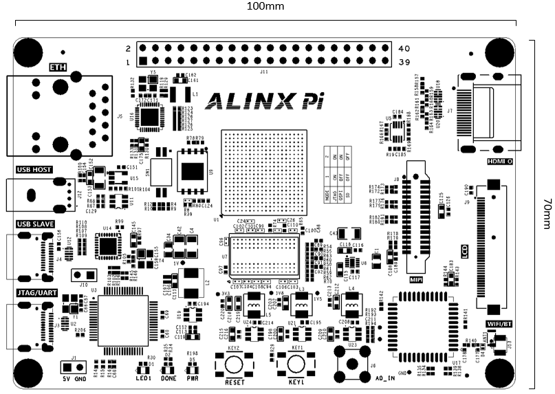
Figure 2.1.1 – Structural Drawing
Chapter 3 Power Supply
Power input: The development board is powered at 5V, supplied directly through the TYPE-C interface, or alternatively by an external DC5V supply. The power design of the board is shown in the following diagram:
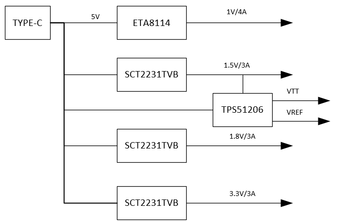
Figure 3.1.1 – Power Interface Section in the Schematic
The board is powered by +5V, which is converted by four DC/DC power chips into four rails: +3.3V, +1.5V, +1.8V and +1.0V. Three of the outputs can deliver up to 3A, and the core supply can provide up to 4A. The 1.5V rail generates the VTT and VREF voltages required by the DDR3 through the TI TPS51206. The function of each power rail is shown in the table below:
| Power Rail | Function |
| +3.3V | ZYNQ VCCIO, Ethernet, JTAG, HDMI, NOR flash, WIFI/BT module and SD card |
| +1.8V | ZYNQ auxiliary voltage, ZYNQ PLL, ZYNQ Bank501 VCCIO, Ethernet, USB2.0 |
| +1.0V | ZYNQ core voltage |
| +1.5V | DDR3, ZYNQ Bank502 |
| VREF, VTT | DDR3 |
Table 3.1.1 – Power Rail Allocation
Because the PS and PL power domains of the ZYNQ have power-up sequencing requirements, the circuit design follows the ZYNQ power requirements, with the power-on sequence of 1.0V -> 1.8V -> 1.5V -> 3.3V.
When designing the PCB, we used an 8-layer board with dedicated power and ground planes, giving the board's power supply excellent stability. Test points for each power rail are reserved on the PCB so that users can verify the voltages on the board.
Chapter 4 ZYNQ7000
The development board uses a Xilinx Zynq-7000 series chip, model XC7Z010-1CLG400C. The PS of the chip integrates two ARM Cortex™-A9 processors, AMBA® interconnect, internal memory, external memory interfaces and peripherals. These peripherals mainly include USB bus interfaces, Ethernet interfaces, SD/SDIO interfaces, I2C bus interfaces, CAN bus interfaces, UART interfaces and GPIO. The PS can run independently and boots at power-on or reset. The overall block diagram of the ZYNQ7000 chip is shown in Figure 4.1.1:
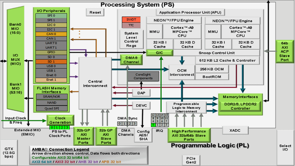
Figure 4.1.1 – ZYNQ7000 Chip Block Diagram
The main parameters of the PS are as follows:
Application processor based on dual-core ARM Cortex-A9
32KB L1 instruction and data cache per CPU, 512KB L2 cache shared by the two CPUs
On-chip boot ROM and 256KB on-chip RAM
External memory interface supporting 16/32-bit DDR2 and DDR3
Two Gigabit Ethernet controllers supporting: scatter-gather DMA, GMII, RGMII, SGMII interfaces
Two USB2.0 OTG interfaces, each supporting up to 12 nodes
Two CAN2.0B bus interfaces
Two SD card, SDIO, MMC-compatible controllers
2 SPI, 2 UARTs, 2 I2C interfaces
4 groups of 32-bit GPIO: 54 (32+22) used as PS system IO, 64 connected to PL
High-bandwidth connections within the PS and from PS to PL
The main parameters of the PL are as follows:
Logic Cells: 28K
LUTs: 17600
Flip-flops: 35200
18x25 MACCs: 80
Block RAM: 2.1Mb
Two AD converters that can measure on-chip voltage, temperature and up to 17 external differential input channels at 1MBPS
The XC7Z010-1CLG400C chip is in a BGA package with 400 pins and a 0.8mm pin pitch. A note on BGA pins: when a BGA-packaged chip is used, pin names take the form of letter+number, such as E3, G3, etc. Therefore, when you look at the schematic, pins in the letter+number format represent BGA pins.
4.1 JTAG Interface
First, let's look at the JTAG debug interface of the PI-ZN010-F1-1 development board. The JTAG download and debug circuit is integrated on the board, so users do not need to purchase an additional Xilinx downloader. A single USB cable is enough for ZYNQ development and debugging. On the PI-ZN010-F1-1, an FTDI USB bridge chip FT2232HL is used to provide data communication between the PC's USB and the ZYNQ's JTAG debug signals TCK, TDO, TMS and TDI, as well as UART debug functionality.
On the PI-ZN010-F1-1 development board, the JTAG interface takes the form of a USB interface. Users can connect the PC to the JTAG interface with the USB cable provided by us to debug the ZYNQ system.
4.2 FPGA Power Supply System
Next, we describe the power design of the PI-ZN010-F1-1. The power supply of the ZYNQ chip is divided into the PS and the PL parts, which operate independently. Both the PS power and the PL power have power-up sequencing requirements; an incorrect power-up sequence may prevent the ARM and FPGA systems from working properly.
The PS power consists of VCCPINT, VCCPAUX, VCCPLL and PS VCCO. VCCPINT is the PS core power pin, connected to 1.0V; VCCPAUX is the PS auxiliary power pin, connected to 1.8V; VCCPLL is the power pin for the PS internal clock PLL, also connected to 1.8V; PS VCCO is the bank voltage, including VCCO_MIO0, VCCO_MIO1 and VCCO_DDR. Depending on the peripherals connected, the supply voltages differ. On the PI-ZN010-F1-1, VCCO_MIO0 is connected to 3.3V, VCCO_MIO1 to 1.8V, and VCCO_DDR to 1.5V. The PS requires the power-up sequence of VCCPINT first, then VCCPAUX and VCCPLL, and finally PS VCCO. The power-down sequence is the reverse.
The PL power consists of VCCINT, VCCBRAM, VCCAUX and VCCO. VCCINT is the FPGA core power pin, connected to 1.0V; VCCBRAM is the FPGA Block RAM power pin, connected to 1.0V; VCCAUX is the FPGA auxiliary power pin, connected to 1.8V; VCCO is the voltage for the PL banks, including BANK13, BANK34 and BANK35. On the PI-ZN010-F1-1, the bank voltage is connected to 3.3V. The PL requires the power-up sequence of VCCINT first, then VCCBRAM, then VCCAUX, and finally VCCO. If VCCINT and VCCBRAM use the same voltage, they can be powered up simultaneously. The power-down sequence is the reverse.
4.3 ZYNQ Boot Configuration
The PI-ZN010-F1-1 development platform supports three boot modes: JTAG debug mode, QSPI FLASH boot mode and SD card boot mode. After power-on, the ZYNQ7010 chip detects the levels of the corresponding MIO pins to determine the boot mode. Users can select different boot modes via the SW1 DIP switch on the board. The SW1 boot mode configuration is shown in Table 4.3.1.
| SW1 | DIP Switch Setting ON/OFF (2:1) | Boot Mode | |
| 0 | 0 | JTAG |
| 0 | 1 | QSPI FLASH | |
| 1 | 1 | SD card | |
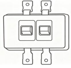
Table 4.3.1 – SW1 Boot Mode Configuration
Chapter 5 Clock Configuration
The PI-ZN010-F1-1 development board provides active clock sources for both the PS and the PL logic, allowing them to work independently.
5.1 PS System Clock Source
The ZYNQ chip receives a 33.333MHz clock input for the PS from the Y2 crystal oscillator on the board. The clock input is connected to the PS_CLK_500 pin of BANK500 on the ZYNQ chip. The clock pin assignment:
| ZYNQ Pin Name | ZYNQ Pin |
| PS_CLK_500 | E7 |
Table 5.1.1 – PS System Clock Source
5.2 PL System Clock Source
The PI-ZN010-F1-1 development board provides a single-ended 50MHz PL system clock source powered at 3.3V. The oscillator output is connected to the FPGA's global clock (MRCC); this GCLK can be used to drive user logic circuits inside the FPGA. PL clock pin assignment:
| ZYNQ Pin Name | ZYNQ Pin |
| IO_L13P_T2_MRCC_34 | N18 |
Table 5.2.1 – PL Clock Pin Assignment
Chapter 6 PS Peripherals
Since the ZYNQ consists of the ARM-based PS and the FPGA-based PL, some peripherals on the board are connected to the PS IO while others are connected to the PL IO. First, we introduce the peripherals connected to the PS.
6.1 QSPI Flash
The development board is equipped with a 128Mbit Quad-SPI FLASH chip, model GD25Q128ESIGR, which uses the 3.3V CMOS voltage standard. Thanks to the non-volatile nature of the QSPI FLASH, it can serve as the system boot device to store the boot images, including the FPGA bit file, ARM application code and other user data files. The specific model and related parameters of the QSPI FLASH are listed in Table 6.1.1.
| Designator | Chip Type | Capacity | Manufacturer |
| U9 | GD25Q128ESIGR | 16M Byte | Giga Device |
Table 6.1.1 – QSPI Flash Model and Parameters
The QSPI FLASH is connected to the GPIO pins of BANK500 in the PS of the ZYNQ chip. In the system design, these PS GPIO pins need to be configured as the QSPI FLASH interface. Figure 6.1.1 shows the hardware connection diagram of the QSPI Flash.
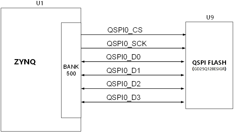
Figure 6.1.1 – QSPI Flash Connection Diagram
FLASH chip pin assignment:
| Signal Name | ZYNQ Pin Name | ZYNQ Pin Number |
| QSPI0_CLK | PS_MIO6_500 | A5 |
| QSPI0_CS | PS_MIO1_500 | A7 |
| QSPI0_D0 | PS_MIO2_500 | B8 |
| QSPI0_D1 | PS_MIO3_500 | D6 |
| QSPI0_D2 | PS_MIO4_500 | B7 |
| QSPI0_D3 | PS_MIO5_500 | A6 |
Table 6.1.2 – QSPI Flash Pin Assignment
6.2 DDR3 DRAM
The PI-ZN010-F1-1 development board is equipped with a Samsung 2Gbit (256MB) DDR3 chip, model K4B2G1646F-BYMA. The DDR bus width is 16 bits. The DDR3 SDRAM can operate at up to 533MHz (data rate 1066Mbps). The DDR3 memory system is connected directly to the memory interface of BANK502 in the ZYNQ processing system (PS). The specific DDR3 SDRAM configuration is shown in Table 6.2.1 below.
| Designator | Chip Type | Capacity | Manufacturer |
| U7 | K4B2G1646F-BYMA | 128M x 16bit | Samsung |
Table 6.2.1 – DDR3 SDRAM Configuration
DDR3 hardware design requires strict attention to signal integrity. In both the circuit and PCB design, we have fully considered matching/termination resistors, trace impedance control and trace length matching to ensure the DDR3 operates reliably at high speed. The hardware connection diagram of the DDR3 DRAM is shown in Figure 6.2.1:
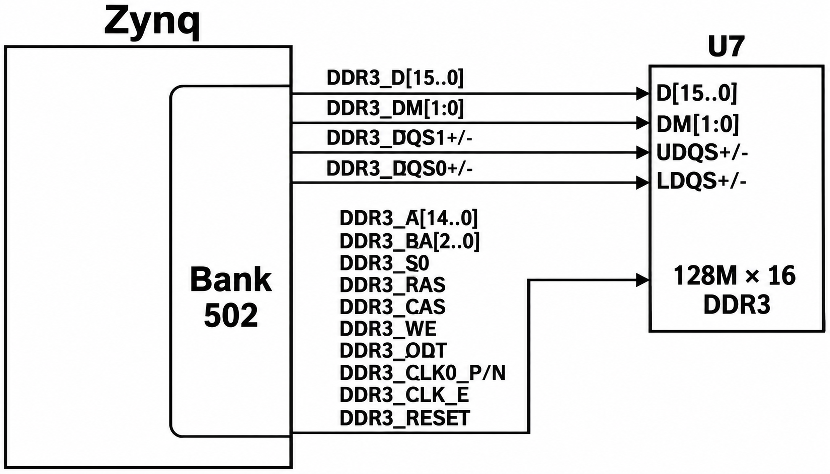
Figure 6.2.1 – DDR3 DRAM Schematic Section
DDR3 DRAM pin assignment:
| Signal Name | ZYNQ Pin Name | ZYNQ Pin Number |
| DDR3_DQS0_P | PS_DDR_DQS_P0_502 | C2 |
| DDR3_DQS0_N | PS_DDR_DQS_N0_502 | B2 |
| DDR3_DQS1_P | PS_DDR_DQS_P1_502 | G2 |
| DDR3_DQS1_N | PS_DDR_DQS_N1_502 | F2 |
| DDR3_DQ[0] | PS_DDR_DQ0_502 | C3 |
| DDR3_DQ[1] | PS_DDR_DQ1_502 | B3 |
| DDR3_DQ[2] | PS_DDR_DQ2_502 | A2 |
| DDR3_DQ[3] | PS_DDR_DQ3_502 | A4 |
| DDR3_DQ[4] | PS_DDR_DQ4_502 | D3 |
| DDR3_DQ[5] | PS_DDR_DQ5_502 | D1 |
| DDR3_DQ[6] | PS_DDR_DQ6_502 | C1 |
| DDR3_DQ[7] | PS_DDR_DQ7_502 | E1 |
| DDR3_DQ[8] | PS_DDR_DQ8_502 | E2 |
| DDR3_DQ[9] | PS_DDR_DQ9_502 | E3 |
| DDR3_DQ[10] | PS_DDR_DQ10_502 | G3 |
| DDR3_DQ[11] | PS_DDR_DQ11_502 | H3 |
| DDR3_DQ[12] | PS_DDR_DQ12_502 | J3 |
| DDR3_DQ[13] | PS_DDR_DQ13_502 | H2 |
| DDR3_DQ[14] | PS_DDR_DQ14_502 | H1 |
| DDR3_DQ[15] | PS_DDR_DQ15_502 | J1 |
| DDR3_DM0 | PS_DDR_DM0_502 | A1 |
| DDR3_DM1 | PS_DDR_DM1_502 | F1 |
| DDR3_A[0] | PS_DDR_A0_502 | N2 |
| DDR3_A[1] | PS_DDR_A1_502 | K2 |
| DDR3_A[2] | PS_DDR_A2_502 | M3 |
| DDR3_A[3] | PS_DDR_A3_502 | K3 |
| DDR3_A[4] | PS_DDR_A4_502 | M4 |
| DDR3_A[5] | PS_DDR_A5_502 | L1 |
| DDR3_A[6] | PS_DDR_A6_502 | L4 |
| DDR3_A[7] | PS_DDR_A7_502 | K4 |
| DDR3_A[8] | PS_DDR_A8_502 | K1 |
| DDR3_A[9] | PS_DDR_A9_502 | J4 |
| DDR3_A[10] | PS_DDR_A10_502 | F5 |
| DDR3_A[11] | PS_DDR_A11_502 | G4 |
| DDR3_A[12] | PS_DDR_A12_502 | E4 |
| DDR3_A[13] | PS_DDR_A13_502 | D4 |
| DDR3_A[14] | PS_DDR_A14_502 | F4 |
| DDR3_BA[0] | PS_DDR_BA0_502 | L5 |
| DDR3_BA[1] | PS_DDR_BA1_502 | R4 |
| DDR3_BA[2] | PS_DDR_BA2_502 | J5 |
| DDR3_S0 | PS_DDR_CS_B_502 | N1 |
| DDR3_RAS | PS_DDR_RAS_B_502 | P4 |
| DDR3_CAS | PS_DDR_CAS_B_502 | P5 |
| DDR3_WE | PS_DDR_WE_B_502 | M5 |
| DDR3_ODT | PS_DDR_ODT_502 | N5 |
| DDR3_RESET | PS_DDR_DRST_B_502 | B4 |
| DDR3_CLK_P | PS_DDR_CKP_502 | L2 |
| DDR3_CLK_N | PS_DDR_CKN_502 | M2 |
| DDR3_CKE | PS_DDR_CKE_502 | N3 |
Table 6.2.2 – DDR3 DRAM Pin Assignment
6.3 Gigabit Ethernet Interface
The PI-ZN010-F1-1 development board provides network communication through the JLSemi JL2121 Ethernet PHY chip. The Ethernet PHY chip is connected to the GPIO interface of BANK501 in the ZYNQ PS. The JL2121 supports 10/100/1000 Mbps data rates and communicates with the MAC layer of the Zynq7000 PS through the RGMII interface. The JL2121 supports MDI/MDIX auto-negotiation, speed auto-negotiation and Master/Slave auto-negotiation, and supports the MDIO bus for PHY register management.
On power-up, the JL2121 detects the level states of certain IO pins to determine its operating mode. Table 6.3.1 describes the default configuration of the GPHY chip after power-on.
| Configuration Pin | Description | Configuration Value |
| ADR[2:0] | MDIO/MDC mode PHY address | PHY address is 001 |
| RX Delay | RX clock 2ns delay | Delayed |
| TX Delay | TX clock 2ns delay | Delayed |
Table 6.3.1 – PHY Chip Default Configuration
When connected to Gigabit Ethernet, data transfer between the FPGA and the JL2121 PHY chip takes place over the RGMII bus, with a 125MHz transfer clock; data is sampled on both the rising and falling edges of the clock.
When connected to 100M Ethernet, data transfer between the FPGA and the JL2121 PHY chip takes place over the RGMII bus, with a 25MHz transfer clock; data is sampled on both the rising and falling edges of the clock.
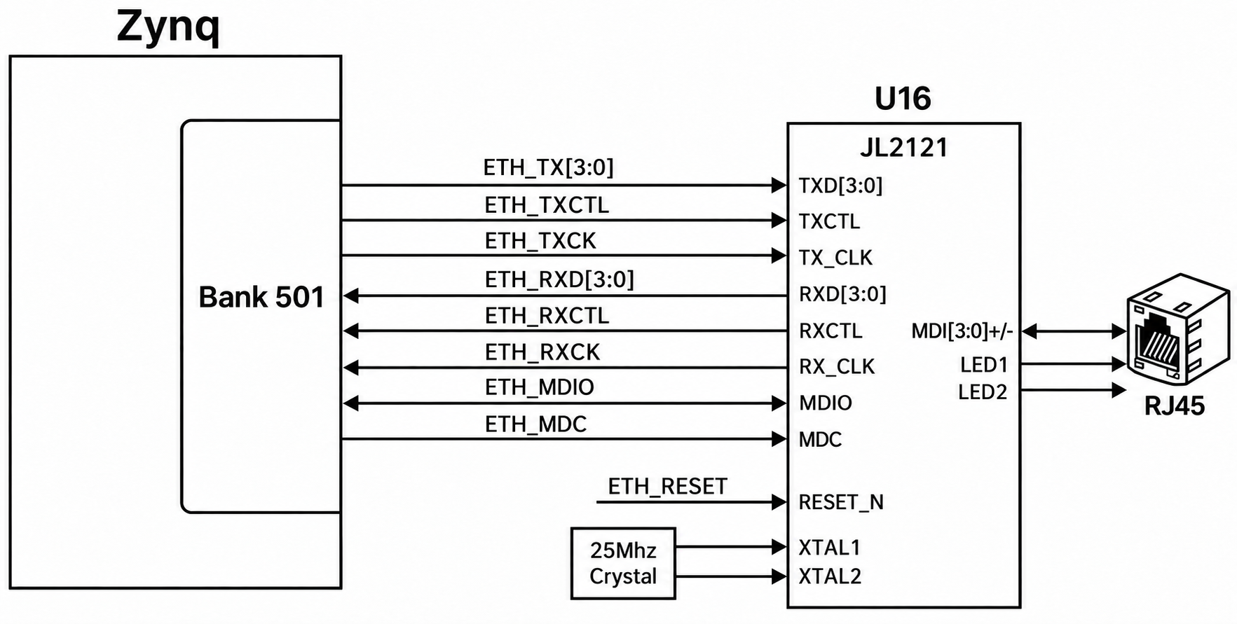
Figure 6.3.1 – FPGA-to-PHY Connection Diagram
The Ethernet pin assignment is as follows:
| Signal Name | ZYNQ Pin Name | ZYNQ Pin Number | Remark |
| ETH_TXCK | PS_MIO16_501 | A19 | RGMII transmit clock |
| ETH_TXD0 | PS_MIO17_501 | E14 | Transmit data bit0 |
| ETH_TXD1 | PS_MIO18_501 | B18 | Transmit data bit1 |
| ETH_TXD2 | PS_MIO19_501 | D10 | Transmit data bit2 |
| ETH_TXD3 | PS_MIO20_501 | A17 | Transmit data bit3 |
| ETH_TXCTL | PS_MIO21_501 | F14 | Transmit enable signal |
| ETH_RXCK | PS_MIO22_501 | B17 | RGMII receive clock |
| ETH_RXD0 | PS_MIO23_501 | D11 | Receive data bit0 |
| ETH_RXD1 | PS_MIO24_501 | A16 | Receive data bit1 |
| ETH_RXD2 | PS_MIO25_501 | F15 | Receive data bit2 |
| ETH_RXD3 | PS_MIO26_501 | A15 | Receive data bit3 |
| ETH_RXCTL | PS_MIO27_501 | D13 | Receive data valid signal |
| ETH_MDC | PS_MIO52_501 | C10 | MDIO management clock |
| ETH_MDIO | PS_MIO53_501 | C11 | MDIO management data |
| ETH_RESET | PS_MIO49_501 | C12 | Ethernet reset |
Table 6.3.2 – Ethernet Pin Assignment
6.4 USB2.0
The PI-ZN010-F1-1 uses a 1.8V high-speed USB3320C-EZK USB2.0 transceiver that supports the ULPI standard interface. The USB bus interface of the ZYNQ is connected to the USB3320C-EZK transceiver to achieve high-speed USB2.0 data communication in both Host and Slave modes. The USB data and control signals of the USB3320C are connected to the IO pins of BANK501 in the ZYNQ PS, and a 24MHz crystal oscillator provides the system clock for the USB3320C.
The board provides two USB interfaces for users: one Host USB port and one Slave USB port. They are a USB2.0 interface (USB Type A) and a TYPE-C interface, making it convenient to connect different USB peripherals. Users can switch between Host and Slave modes via the J10 jumper on the board. Table 6.4.1 describes the mode switching:
| J10 Status | USB Mode | Description |
| Jumper installed | HOST mode | The board acts as the host device; the USB port connects to slave peripherals such as a mouse, keyboard and USB flash drive |
| No jumper | OTG/Slave mode | The board acts as a slave device; the USB port connects to a PC |
Table 6.4.1 – USB Interface Mode Switching
The connection diagram between the ZYNQ processor and the USB3320C-EZK chip is shown in Figure 6.4.1:
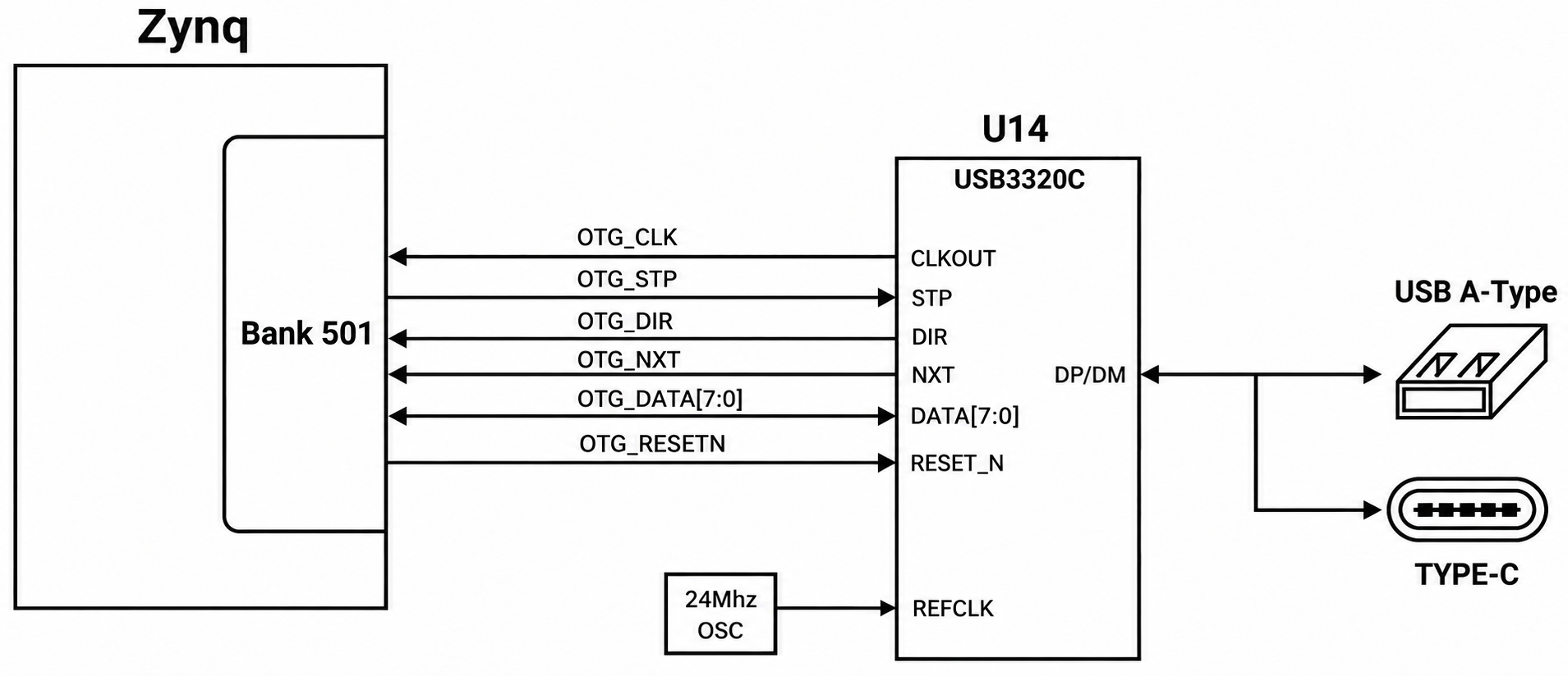
Figure 6.4.1 – Connection Diagram between Zynq7000 and USB Chip
Figure 6.4.2 shows the physical layout of the USB2.0 section. U14 is the USB3320C, J12 is the Host USB interface and J4 is the Slave USB interface. Jumper J10 is used to select Host or Slave mode.
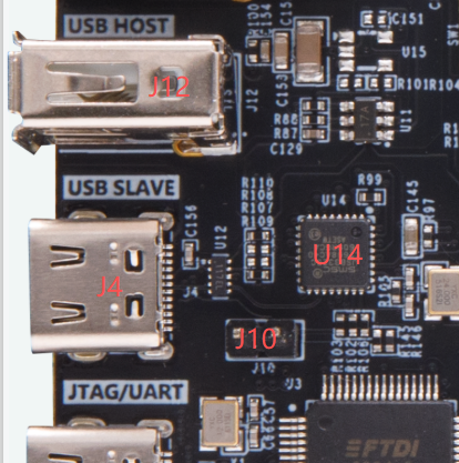
Figure 6.4.2 – USB2.0 Interface Photo
The USB2.0 pin assignment is shown in the table below:
| Signal Name | ZYNQ Pin Name | ZYNQ Pin Number | Remark |
| OTG_DATA4 | PS_MIO28_501 | C16 | USB data bit4 |
| OTG_DIR | PS_MIO29_501 | C13 | USB data direction signal |
| OTG_STP | PS_MIO30_501 | C15 | USB stop signal |
| OTG_NXT | PS_MIO31_501 | E16 | USB next data signal |
| OTG_DATA0 | PS_MIO32_501 | A14 | USB data bit0 |
| OTG_DATA1 | PS_MIO33_501 | D15 | USB data bit1 |
| OTG_DATA2 | PS_MIO34_501 | A12 | USB data bit2 |
| OTG_DATA3 | PS_MIO35_501 | F12 | USB data bit3 |
| OTG_CLK | PS_MIO36_501 | A11 | USB clock signal |
| OTG_DATA5 | PS_MIO37_501 | A10 | USB data bit5 |
| OTG_DATA6 | PS_MIO38_501 | E13 | USB data bit6 |
| OTG_DATA7 | PS_MIO39_501 | C18 | USB data bit7 |
| OTG_RESETN | PS_MIO1_501 | B9 | USB reset signal |
Table 6.4.2 – USB2.0 Pin Assignment
6.5 USB-to-UART
The PI-ZN010-F1-1 development board uses the FTDI FT2232HL USB-to-JTAG and UART chip, with a TYPE-C USB interface. Users can connect to a PC with a TYPE-C cable for serial communication.
The UART TX/RX signals are connected to the signals of BANK501 in the ZYNQ PS. Since the VCCMIO of this bank is set to 1.8V while the data level of the FT2232HL is 3.3V, we use the UM3202V level-shifting chip to connect them. The connection diagram between the FT2232HL and the ZYNQ is shown in Figure 6.5.1:
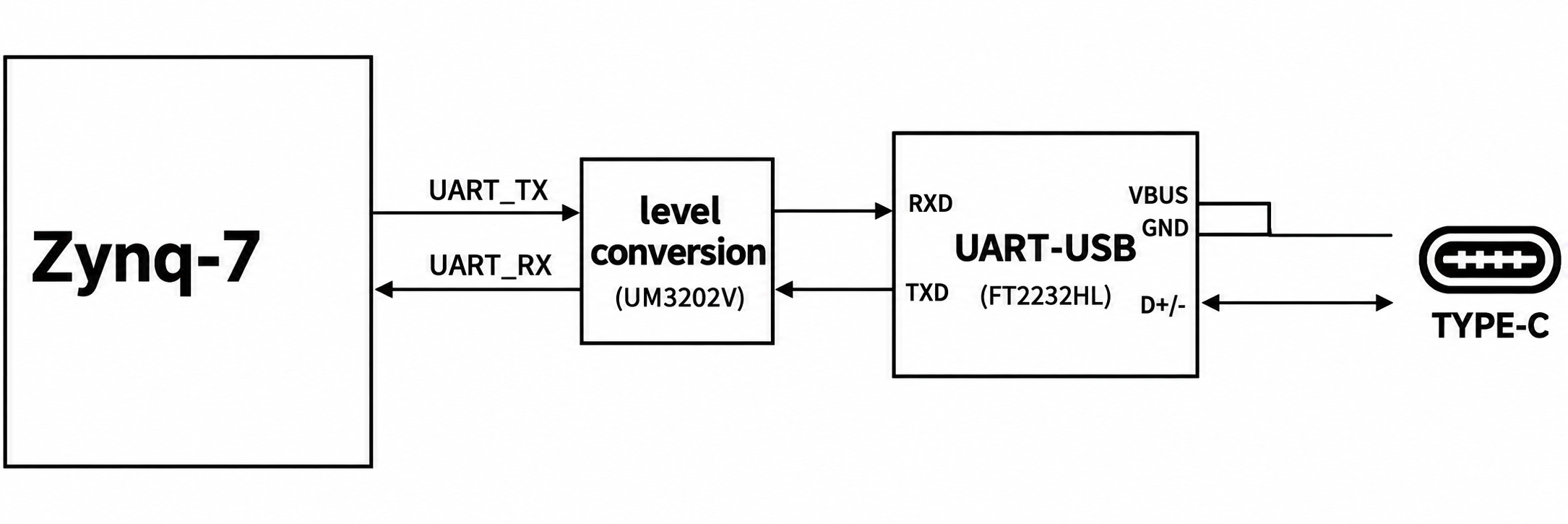
Figure 6.5.1 – FT2232HL Connection Diagram
UART pin assignment:
| Signal Name | ZYNQ Pin Name | ZYNQ Pin Number | Remark |
| UART_TX | PS_MIO47_501 | B14 | UART data output |
| UART_RX | PS_MIO46_501 | D16 | UART data input |
Table 6.5.1 – UART Pin Assignment
FTDI provides Virtual COM Port (VCP) drivers for the host PC. These drivers allow the FT2232HL USB-UART bridge device to appear as a COM port in communication application software (e.g., TeraTerm or HyperTerminal). The VCP device driver must be installed before the PC host can establish communication with the PI-ZN010-F1-1 development board.
6.6 SD Card Slot
The PI-ZN010-F1-1 development board includes a Micro SD card interface, giving users access to SD card storage for storing the ZYNQ chip's BOOT program, Linux operating system kernel, file system and other user data files.
The SDIO signals are connected to the IO signals of BANK501 in the ZYNQ PS. Since the VCCMIO of this bank is set to 1.8V while the SD card data level is 3.3V, we use the TXS02612 level translator to connect them. The schematic of the Zynq7000 PS and the SD card connector is shown in Figure 6.6.1.
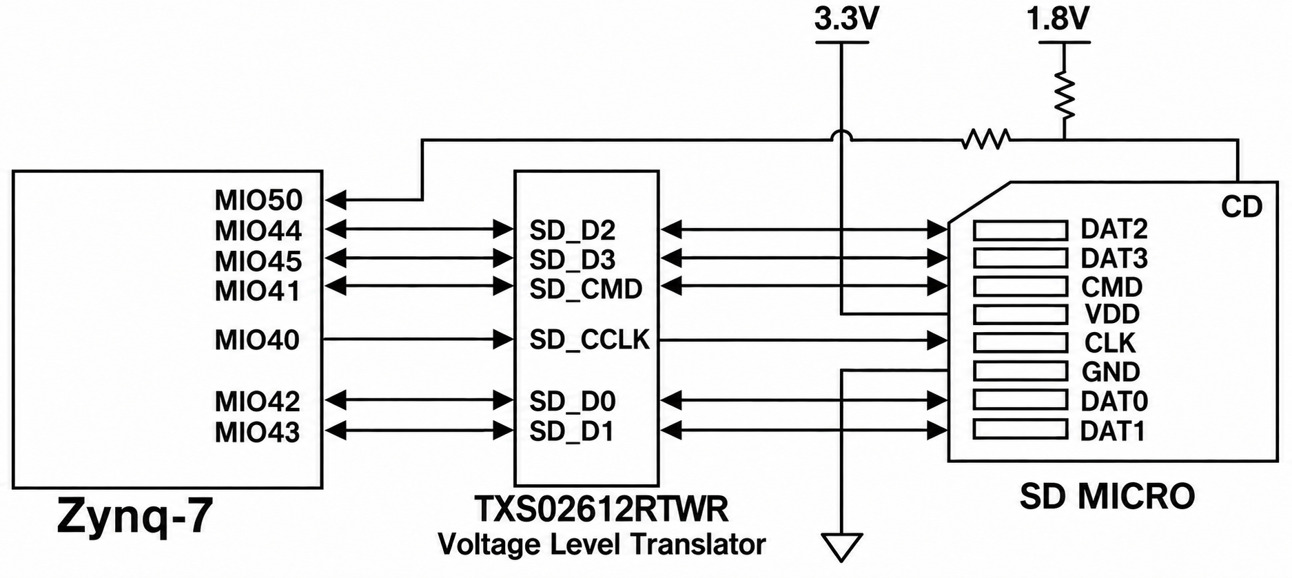
Figure 6.6.1 – SD Card Connection Diagram
SD card slot pin assignment:
| Signal Name | ZYNQ Pin Name | ZYNQ Pin Number | Remark |
| SD0_CLK | PS_MIO40 | D14 | SD clock signal |
| SD0_CMD | PS_MIO41 | C17 | SD command signal |
| SD0_D0 | PS_MIO42 | E12 | SD data bit0 |
| SD0_D1 | PS_MIO43 | A9 | SD data bit1 |
| SD0_D2 | PS_MIO44 | F13 | SD data bit2 |
| SD0_D3 | PS_MIO45 | B15 | SD data bit3 |
| SD0_CD | PS_MIO50 | B13 | SD card insertion signal |
Table 6.6.1 – SD Card Slot Pin Assignment
6.7 WIFI/BT Module
The PI-ZN010-F1-1 development board has an onboard WIFI/BT module, model Quectel FCS961K-L, supporting IEEE 802.11b/g/n/ax protocols. The module supports single-band Wi-Fi 2.4GHz and BLE 5.2, with an SDIO 2.0 interface. Users can develop and use it as needed.
WIFI/BT pin assignment:
| Signal Name | ZYNQ Pin Name | ZYNQ Pin Number | Remark |
| SD1_D0 | PS_MIO10_500 | E9 | SDIO data bit 0 |
| SD1_D1 | PS_MIO13_500 | E8 | SDIO data bit 1 |
| SD1_D2 | PS_MIO14_500 | C5 | SDIO data bit 2 |
| SD1_D3 | PS_MIO15_500 | C8 | SDIO data bit 3 |
| SD1_CLK | PS_MIO12_500 | D9 | SDIO clock |
| SD1_CMD | PS_MIO11_500 | C6 | SDIO command |
| WIFI_CHIP_EN | PS_MIO9_500 | B5 | Module enable |
| BT_TXD | IO_0_35 | G14 | Bluetooth UART transmit |
| BT_RXD | IO_25_35 | J15 | Bluetooth UART receive |
Table 6.7.1 – WIFI/BT Pin Assignment
6.8 AD Input Interface
The PI-ZN010-F1-1 development board is equipped with one AD input interface for acquiring external analog signals and performing AD conversion. An SMA connector is used as the input; the input signal is converted into a differential signal and fed into the ZYNQ. The design diagram of the AD acquisition circuit is shown in Figure 6.8.1 below:
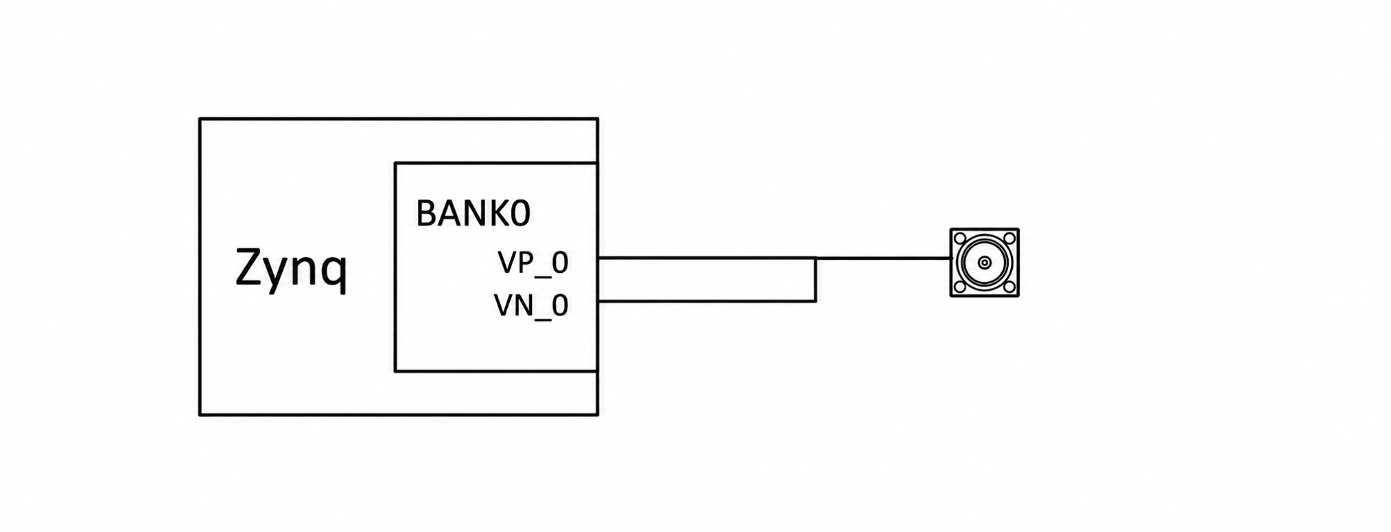
Figure 6.8.1 – AD Acquisition Circuit Design Diagram
ZYNQ pin assignment of the AD acquisition circuit:
| Signal Name | ZYNQ Pin Name | ZYNQ Pin Number | Remark |
| ADC_P | VP_0 | K9 | AD_IN_P |
| ADC_N | VN_0 | L10 | AD_IN_N |
Table 6.8.1 – ZYNQ Pin Assignment of the AD Acquisition Circuit
Chapter 7 PL Peripherals
Next, we introduce the peripherals connected to the PL (FPGA logic).
7.1 HDMI Interface
HDMI stands for High-Definition Multimedia Interface. On the PI-ZN010-F1-1, the HDMI signals are connected to BANK35 of the ZYNQ PL. The differential signals and clock of the HDMI interface are connected directly through the FPGA's differential IO. Inside the FPGA, the HDMI differential signals are converted to parallel and then encoded/decoded, implementing a digital video output transmission solution with support for up to 1080P@60Hz output.
When the board acts as an HDMI source (HDMI OUT), it must provide +5V power to the HDMI display device. In addition, the HDMI source reads the EDID information of the HDMI display device via the IIC bus. The FPGA pin level is 3.3V, while the HDMI level is +5V, so we need the UM3202V level-shifting chip to connect them. The pin assignment of the HDMI interface is shown in the table below:
| Signal Name | ZYNQ Pin Name | ZYNQ Pin Number | Remark |
| HDMI_CLK_P | IO_L7P_T1_AD2P_35 | M19 | HDMI clock signal positive |
| HDMI_CLK_N | IO_L7N_T1_AD2N_35 | M20 | HDMI clock signal negative |
| HDMI_D0_P | IO_L9P_T1_DQS_AD3P_35 | L19 | HDMI data 0 positive |
| HDMI_D0_N | IO_L9N_T1_DQS_AD3N_35 | L20 | HDMI data 0 negative |
| HDMI_D1_P | IO_L18P_T2_AD13P_35 | G19 | HDMI data 1 positive |
| HDMI_D1_N | IO_L18N_T2_AD13N_35 | G20 | HDMI data 1 negative |
| HDMI_D2_P | IO_L15P_T2_DQS_AD12P_35 | F19 | HDMI data 2 positive |
| HDMI_D2_N | IO_L15N_T2_DQS_AD12N_35 | F20 | HDMI data 2 negative |
| HDMI_SCL | IO_L24N_T3_34 | P16 | HDMI IIC clock |
| HDMI_SDA | IO_L24P_T3_34 | P15 | HDMI IIC data |
Table 7.1.1 – HDMI Interface Pin Assignment
7.2 LCD Interface
The PI-ZN010-F1-1 development board provides an LCD interface for connecting a 4.3-inch display module. The signals are connected to the BANK34 IO pins of the ZYNQ PL. Table 7.2.1 shows the pin assignment of the LCD interface on the BANK34 IO:
| Signal Name | ZYNQ Pin Name | ZYNQ Pin Number | Remark |
| LCD_R0 | IO_L14P_T2_SRCC_34 | N20 | Bit 0 of LCD red data channel |
| LCD_R1 | IO_L14N_T2_SRCC_34 | P20 | Bit 1 of LCD red data channel |
| LCD_R2 | IO_L15P_T2_DQS_34 | T20 | Bit 2 of LCD red data channel |
| LCD_R3 | IO_L15N_T2_DQS_34 | U20 | Bit 3 of LCD red data channel |
| LCD_R4 | IO_L16P_T2_34 | V20 | Bit 4 of LCD red data channel |
| LCD_R5 | IO_L16N_T2_34 | W20 | Bit 5 of LCD red data channel |
| LCD_R6 | IO_L23N_T3_34 | P18 | Bit 6 of LCD red data channel |
| LCD_R7 | IO_25_34 | T19 | Bit 7 of LCD red data channel |
| LCD_G0 | IO_0_34 | R19 | Bit 0 of LCD green data channel |
| LCD_G1 | IO_L23P_T3_34 | N17 | Bit 1 of LCD green data channel |
| LCD_G2 | IO_L22N_T3_34 | W19 | Bit 2 of LCD green data channel |
| LCD_G3 | IO_L13N_T2_MRCC_34 | P19 | Bit 3 of LCD green data channel |
| LCD_G4 | IO_L22P_T3_34 | W18 | Bit 4 of LCD green data channel |
| LCD_G5 | IO_L19N_T3_VREF_34 | R17 | Bit 5 of LCD green data channel |
| LCD_G6 | IO_L9N_T1_DQS_34 | U17 | Bit 6 of LCD green data channel |
| LCD_G7 | IO_L18N_T2_34 | W16 | Bit 7 of LCD green data channel |
| LCD_B0 | IO_L18P_T2_34 | V16 | Bit 0 of LCD blue data channel |
| LCD_B1 | IO_L10N_T1_34 | W15 | Bit 1 of LCD blue data channel |
| LCD_B2 | IO_L10P_T1_34 | V15 | Bit 2 of LCD blue data channel |
| LCD_B3 | IO_L9P_T1_DQS_34 | T16 | Bit 3 of LCD blue data channel |
| LCD_B4 | IO_L3N_T0_DQS_34 | V13 | Bit 4 of LCD blue data channel |
| LCD_B5 | IO_L4P_T0_34 | V12 | Bit 5 of LCD blue data channel |
| LCD_B6 | IO_L4N_T0_34 | W13 | Bit 6 of LCD blue data channel |
| LCD_B7 | IO_L2N_T0_34 | U12 | Bit 7 of LCD blue data channel |
| LCD_CLK | IO_L2P_T0_34 | T12 | LCD clock |
| LCD_HSYNC | IO_L6N_T0_VREF_34 | R14 | LCD horizontal sync |
| LCD_VSYNC | IO_L1P_T0_34 | T11 | LCD vertical sync |
| LCD_DE | IO_L1N_T0_34 | T10 | LCD data enable |
| LCD_BL | IO_L5P_T0_34 | T14 | LCD backlight enable |
| TP_RST | IO_L3P_T0_DQS_PUDC_B_34 | U13 | LCD touchscreen reset |
| TP_SDA | IO_L11P_T1_SRCC_34 | U14 | LCD touchscreen I2C data |
| TP_SCL | IO_L5N_T0_34 | T15 | LCD touchscreen I2C clock |
| TP_INTR | IO_L19P_T2_34 | R16 | LCD touchscreen interrupt |
Table 7.2.1 – LCD Pin Assignment
7.3 MIPI Interface
The PI-ZN010-F1-1 development board includes a MIPI camera interface for connecting our MIPI OV5640 camera module. The MIPI interface signals are connected to the BANK34 and BANK35 IO pins of the ZYNQ PL. Figure 7.3.1 shows the MIPI schematic.
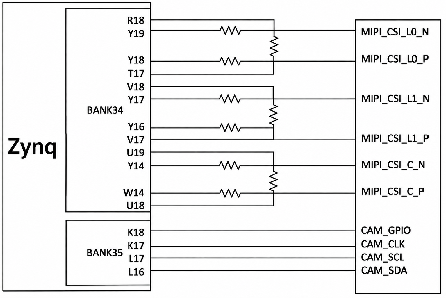
Figure 7.3.1 – MIPI Interface Schematic
MIPI interface pin assignment:
| Signal Name | ZYNQ Pin Name | ZYNQ Pin Number | Remark |
| MIPI_CSI_L0_N | IO_L20N_T3_34 | R18 | LANE0 negative in High Speed mode |
| LP_MIPI_CSI_L0_N | IO_L17N_T2_34 | Y19 | LANE0 negative in Low Power mode |
| LP_MIPI_CSI_L0_P | IO_L17P_T2_34 | Y18 | LANE0 positive in Low Power mode |
| MIPI_CSI_L0_P | IO_L20P_T3_34 | T17 | LANE0 positive in High Speed mode |
| MIPI_CSI_L1_N | IO_L21N_T3_DQS_34 | V18 | LANE1 negative in High Speed mode |
| LP_MIPI_CSI_L1_N | IO_L7N_T1_34 | Y17 | LANE1 negative in Low Power mode |
| LP_MIPI_CSI_L1_P | IO_L7P_T1_34 | Y16 | LANE1 positive in Low Power mode |
| MIPI_CSI_L1_P | IO_L21P_T3_DQS_34 | V17 | LANE1 positive in High Speed mode |
| MIPI_CSI_C_N | IO_L12N_T1_MRCC_34 | U19 | Clock negative in High Speed mode |
| LP_MIPI_CSI_C_N | IO_L8N_T1_34 | Y14 | Clock negative in Low Power mode |
| LP_MIPI_CSI_C_P | IO_L8P_T1_34 | W14 | Clock positive in Low Power mode |
| MIPI_CSI_C_P | IO_L12P_T1_MRCC_34 | U18 | Clock positive in High Speed mode |
| CAM_GPIO | IO_L12N_T1_MRCC_35 | K18 | Camera GPIO control |
| CAM_CLK | IO_L12P_T1_MRCC_35 | K17 | Camera clock input |
| CAM_SCL | IO_L11N_T1_SRCC_35 | L17 | Camera I2C clock |
| CAM_SDA | IO_L11P_T1_SRCC_35 | L16 | Camera I2C data |
Table 7.3.1 – MIPI Pin Assignment
7.4 Expansion Connector J11
The J11 expansion connector is a 40-pin, 2.54mm dual-row connector that allows users to expand with more peripherals and interfaces. The modules currently provided by ALINX include: ADDA module, LCD module, Gigabit Ethernet module, audio input/output module, matrix keyboard module and 500W dual-lens vision camera module. The expansion connector provides 1x 5V power, 2x 3.3V power, 3x ground and 34x IO pins. The IO signals are connected to BANK35 of the ZYNQ PL at 3.3V level. On the PCB, the P and N traces of the expansion connector are routed as differential pairs with a controlled differential impedance of 100 ohms. Do not connect 5V devices directly, as this may damage the FPGA. If you need to connect 5V devices, use a level-shifting chip.
J11 expansion connector pin assignment:
| J11 Pin | Signal Name | ZYNQ Pin Name | ZYNQ Pin Number |
| PIN1 | GND | -- | -- |
| PIN2 | +5V | -- | -- |
| PIN3 | EX_IO1_1N | IO_L6N_T0_VREF_35 | F17 |
| PIN4 | EX_IO1_1P | IO_L6P_T0_35 | F16 |
| PIN5 | EX_IO1_2N | IO_L2N_T0_AD8N_35 | A20 |
| PIN6 | EX_IO1_2P | IO_L2P_T0_AD8P_35 | B19 |
| PIN7 | EX_IO1_3N | IO_L3N_T0_DQS_AD1N_35 | D18 |
| PIN8 | EX_IO1_3P | IO_L3P_T0_DQS_AD1P_35 | E17 |
| PIN9 | EX_IO1_4N | IO_L5N_T0_AD9N_35 | E19 |
| PIN10 | EX_IO1_4P | IO_L5P_T0_AD9P_35 | E18 |
| PIN11 | EX_IO1_5N | IO_L1N_T0_AD0N_35 | B20 |
| PIN12 | EX_IO1_5P | IO_L1P_T0_AD0P_35 | C20 |
| PIN13 | EX_IO1_6N | IO_L17N_T2_AD5N_35 | H20 |
| PIN14 | EX_IO1_6P | IO_L17P_T2_AD5P_35 | J20 |
| PIN15 | EX_IO1_7N | IO_L4N_T0_35 | D20 |
| PIN16 | EX_IO1_7P | IO_L4P_T0_35 | D19 |
| PIN17 | EX_IO1_8N | IO_L10N_T1_AD11N_35 | J19 |
| PIN18 | EX_IO1_8P | IO_L10P_T1_AD11P_35 | K19 |
| PIN19 | EX_IO1_9N | IO_L22N_T3_AD7N_35 | L15 |
| PIN20 | EX_IO1_9P | IO_L22P_T3_AD7P_35 | L14 |
| PIN21 | EX_IO1_10N | IO_L16N_T2_35 | G18 |
| PIN22 | EX_IO1_10P | IO_L16P_T2_35 | G17 |
| PIN23 | EX_IO1_11N | IO_L13N_T2_MRCC_35 | H17 |
| PIN24 | EX_IO1_11P | IO_L13P_T2_MRCC_35 | H16 |
| PIN25 | EX_IO1_12N | IO_L19N_T3_VREF_35 | G15 |
| PIN26 | EX_IO1_12P | IO_L19P_T3_35 | H15 |
| PIN27 | EX_IO1_13N | IO_L14N_T2_AD4N_SRCC_35 | H18 |
| PIN28 | EX_IO1_13P | IO_L14P_T2_AD4P_SRCC_35 | J18 |
| PIN29 | EX_IO1_14N | IO_L20N_T3_AD6N_35 | J14 |
| PIN30 | EX_IO1_14P | IO_L20P_T3_AD6P_35 | K14 |
| PIN31 | EX_IO1_15N | IO_L8N_T1_AD10N_35 | M18 |
| PIN32 | EX_IO1_15P | IO_L8P_T1_AD10P_35 | M17 |
| PIN33 | EX_IO1_16N | IO_L21N_T3_DQS_AD14N_35 | N16 |
| PIN34 | EX_IO1_16P | IO_L21P_T3_DQS_AD14P_35 | N15 |
| PIN35 | EX_IO1_17N | IO_L23N_T3_35 | M15 |
| PIN36 | EX_IO1_17P | IO_L23P_T3_35 | M14 |
| PIN37 | GND | -- | -- |
| PIN38 | GND | -- | -- |
| PIN39 | +3.3V | -- | -- |
| PIN40 | +3.3V | -- | -- |
Table 7.4.1 – J11 Expansion Connector Pin Assignment
7.5 User LED
On the PI-ZN010-F1-1 development board, one LED is connected to the BANK35 IO of the PL. Users can use this LED to debug programs. When the BANK35 IO is high, the LED is off; when the BANK35 IO is low, the LED lights up. The connection diagram between the ZYNQ BANK35 IO and the LED is shown in Figure 7.5.1:
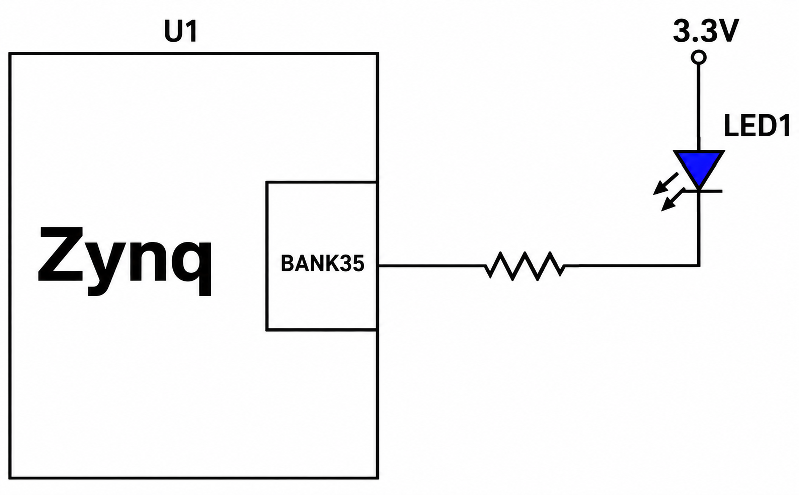
Figure 7.5.1 – Zynq-7000 to LED Connection Diagram
PS LED pin assignment:
| Signal Name | ZYNQ Pin Name | ZYNQ Pin Number | Remark |
| LED1 | IO_L24P_T3_AD15P_35 | K16 | PL LED1 |
Table 7.5.1 – PL LED Pin Assignment
7.6 User Button
On the PI-ZN010-F1-1 development board, one user button is connected to the BANK35 IO of the PL. Users can use this button to test input signals and interrupt triggering. In the design, when the button is pressed, the signal level at the ZYNQ BANK35 IO goes low; when it is not pressed, the signal is high. The connection diagram between the ZYNQ BANK35 IO and the button is shown in Figure 7.6.1:
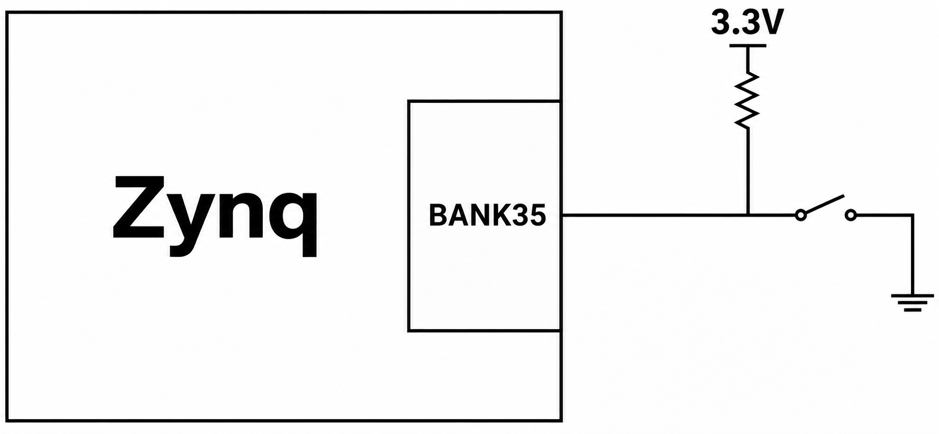
Figure 7.6.1 – Zynq-7000 to Button Connection Diagram
Button pin assignment:
| Signal Name | ZYNQ Pin Name | ZYNQ Pin Number | Remark |
| KEY1 | IO_L24N_T3_AD15N_35 | J16 | PL KEY1 |
Table 7.6.1 – Button Pin Assignment
Appendix: List of Abbreviations
| Abbreviation | Full English Name | Description |
| PS | Processor System | The processing subsystem in an SoC, typically including CPU cores, memory controllers, and peripheral interfaces for running software and operating systems. |
| PL | Programmable Logic | User-configurable FPGA logic resources used to implement custom digital circuits, interface controllers, and hardware acceleration functions. |
| SOC | System on Chip | An integrated circuit that combines processors, memory controllers, peripheral interfaces, and other system functions on a single chip. |
| DDR3 | Double Data Rate 3 SDRAM | A third-generation synchronous dynamic memory technology that transfers data on both edges of the clock signal and is commonly used as system memory. |
| eMMC | Embedded Multi Media Card | An embedded non-volatile storage device that integrates NAND Flash memory and a storage controller in a single package. |
| QSPI | Quad Serial Peripheral Interface | A high-speed serial interface that uses four data lines and is commonly used to connect NOR Flash devices for boot or configuration storage. |
| GTP | Gigabit Transceiver | A high-speed serial transceiver integrated in an FPGA for transmitting and receiving data at multi-gigabit rates. |
| UART | Universal Asynchronous Receiver/Transmitter | An asynchronous serial communication interface that transmits and receives data through TX and RX signal lines. |
| HDMI | High-Definition Multimedia Interface | A digital multimedia interface used to transmit high-definition video and audio signals between source and display devices. |
| PCIe | Peripheral Component Interconnect Express | A high-speed serial expansion bus standard used for communication between processors and devices such as FPGAs, GPUs, and SSDs. |
| USB | Universal Serial Bus | A standard serial interface used for data communication, peripheral connection, and power delivery between electronic devices. |
| JTAG | Joint Test Action Group | A standardized interface used for device testing, boundary scan, FPGA programming, and processor or system debugging. |
| SFP | Small Form-factor Pluggable | A compact, hot-pluggable transceiver interface used for optical or electrical network communication. |
| MIO | Multiplexed I/O | Multiplexed processor I/O pins in an SoC that can be configured for functions such as UART, I2C, SPI, or GPIO. |
| GPHY | Gigabit Ethernet PHY | A Gigabit Ethernet physical-layer transceiver that converts digital Ethernet data into electrical signals for transmission over a physical network medium. |
| I2C | Inter-Integrated Circuit | A two-wire serial communication bus using SDA and SCL lines, commonly used to connect sensors, EEPROMs, and peripheral devices. |
| RGMII | Reduced Gigabit Media Independent Interface | A reduced-pin-count interface between an Ethernet MAC and PHY that supports 10, 100, and 1000 Mbps Ethernet communication. |
| RMII | Reduced Media Independent Interface | A reduced-pin-count interface between an Ethernet MAC and PHY, mainly used for 10 and 100 Mbps Ethernet communication. |
| LED | Light Emitting Diode | A semiconductor device that emits light when electrically driven and is commonly used for power, status, and fault indication. |
| LVDS | Low-Voltage Differential Signaling | A high-speed differential signaling standard that provides low power consumption, low noise, and strong resistance to electromagnetic interference. |
Contact information
Alinx Electronic Limited
Company Website: www.en.alinx.com
Service Hotline: +86 21 67676997
Technical Support:technical@alinx.com