
Appearance
AXW48 User Manual

Alinx Electronic Limited
Company Website: www.en.alinx.com
Service Hotline: +86 21 67676997
Technical Support : technical@alinx.com
Document Information
| Item | Content |
| Document Name | Product Manual |
| Product Model | AXW48 |
| Document Version | V1.0 |
| Prepared by | Alinx Electronic Limited |
| Release Date | 2026.10.26 |
Document Revision History
| Version | Date | Section | Revision Summary |
| V1.0 | 2026.10.26 | All | Initial Release |
Part 1: Introduction
1.1 Product Description
The ZYNQ chip on the AXW48 is based on Xilinx's Zynq™ UltraScale+™ RFSoC Gen3 series XCZU48DR-L2FSVG1517I.
The AXW48 uses 8 Micron DDR4 chips, model MT40A512M16LY-062E IT:E. Four DDR4 chips are mounted on the PS side, forming a 64-bit data bus width, and four DDR4 chips are mounted on the PL side, also forming a 64-bit data bus width. The maximum operating data rate of the DDR4 is 2400 Mb/s, used for high-performance data processing and storage. In addition, one SD card slot is routed out for storing the file system and other user data files. The AXW48 has 4 onboard QSFP connectors to provide optical ports, enabling high-speed data to be processed efficiently in parallel with analog and digital conversion. The PS side expands 2 USB 3.0 ports, one Display interface, one OLED, one SYZYGY connector, and one PMOD connector. Meanwhile, the PS side also expands one 10/100/1000 Ethernet port.
The AXW48 board brings out 8 ADC and 8 DAC ports. The AXW48 with the ZU48DR FPGA is supported by 8 14-bit ADC ports with a sampling rate of 5 GSPS and 8 14-bit DAC ports with a sampling rate of 9.85 GSPS. The ADC and DAC ports use the high-performance RF connector SMA-KHDC16.
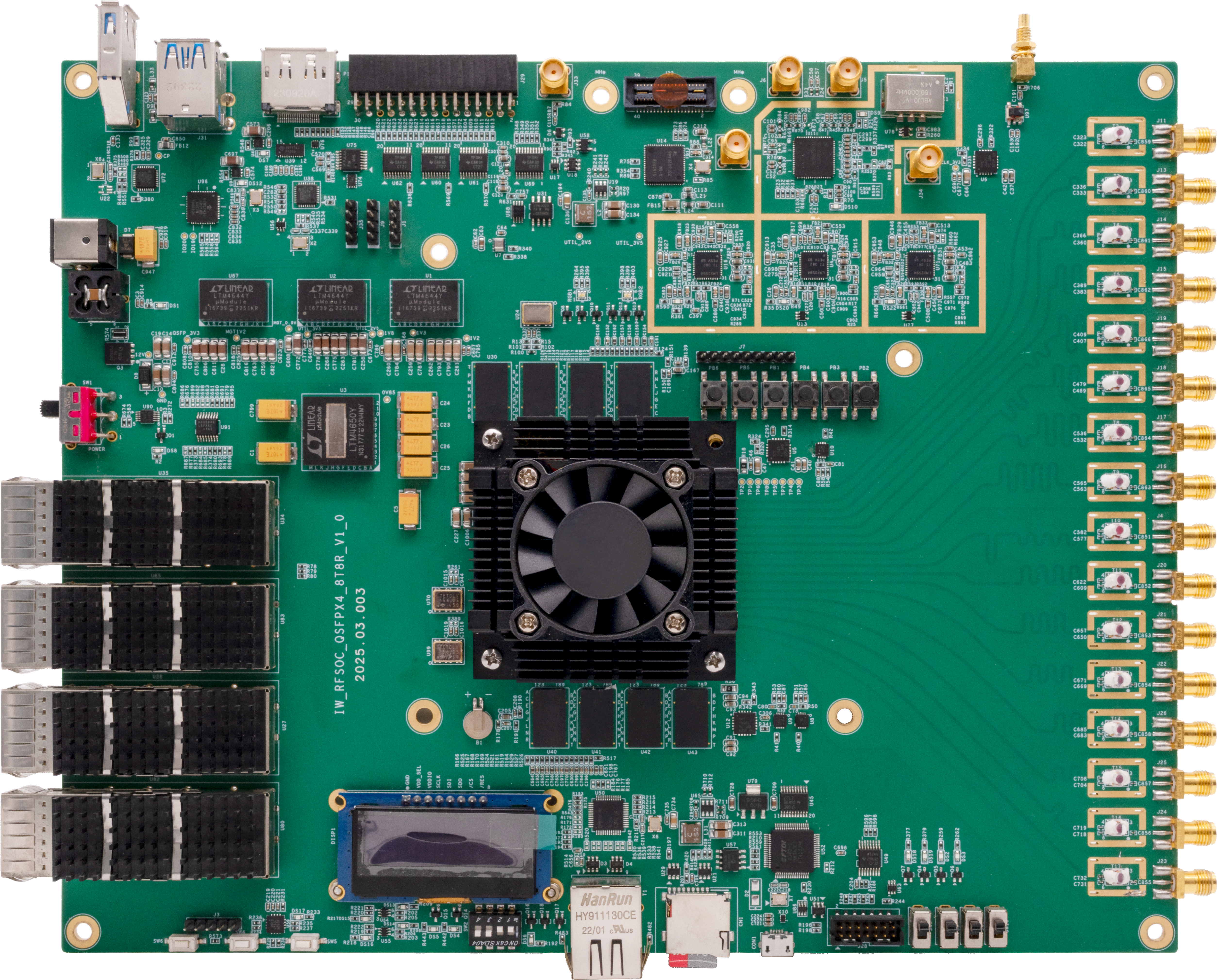
Figure 1.1.1-AXW48 (Top View)
1.2 ZYNQ Chip
The AXW48 uses the Xilinx Zynq™ UltraScale+™ RFSoC Gen3 series chip, model XCZU48DR-L2FSVG1517I. The programmable logic section provides FPGA resources for high-throughput digital signal processing (DSP) and IP cores, such as digital up/down conversion (DUC/DDC) kernels. FPGA acceleration is easier to implement through the software-defined radio development framework application programming interfaces and FPGA infrastructure. This helps get up and running quickly so that you can focus on value-added IP. The FPGA system for common functions such as Fast Fourier Transform (FFT) and Finite Impulse Response (FIR) filters is a good starting point. Use your preferred hardware description language (HDL) to add your own IP blocks to the modular architecture. In addition to the FPGA architecture portion of the system, the Xilinx UltraScale+ RFSoC is also equipped with four onboard application processing units (APUs) and two real-time processing units (RPUs), suitable for applications that require an onboard embedded operating system for standalone operation.
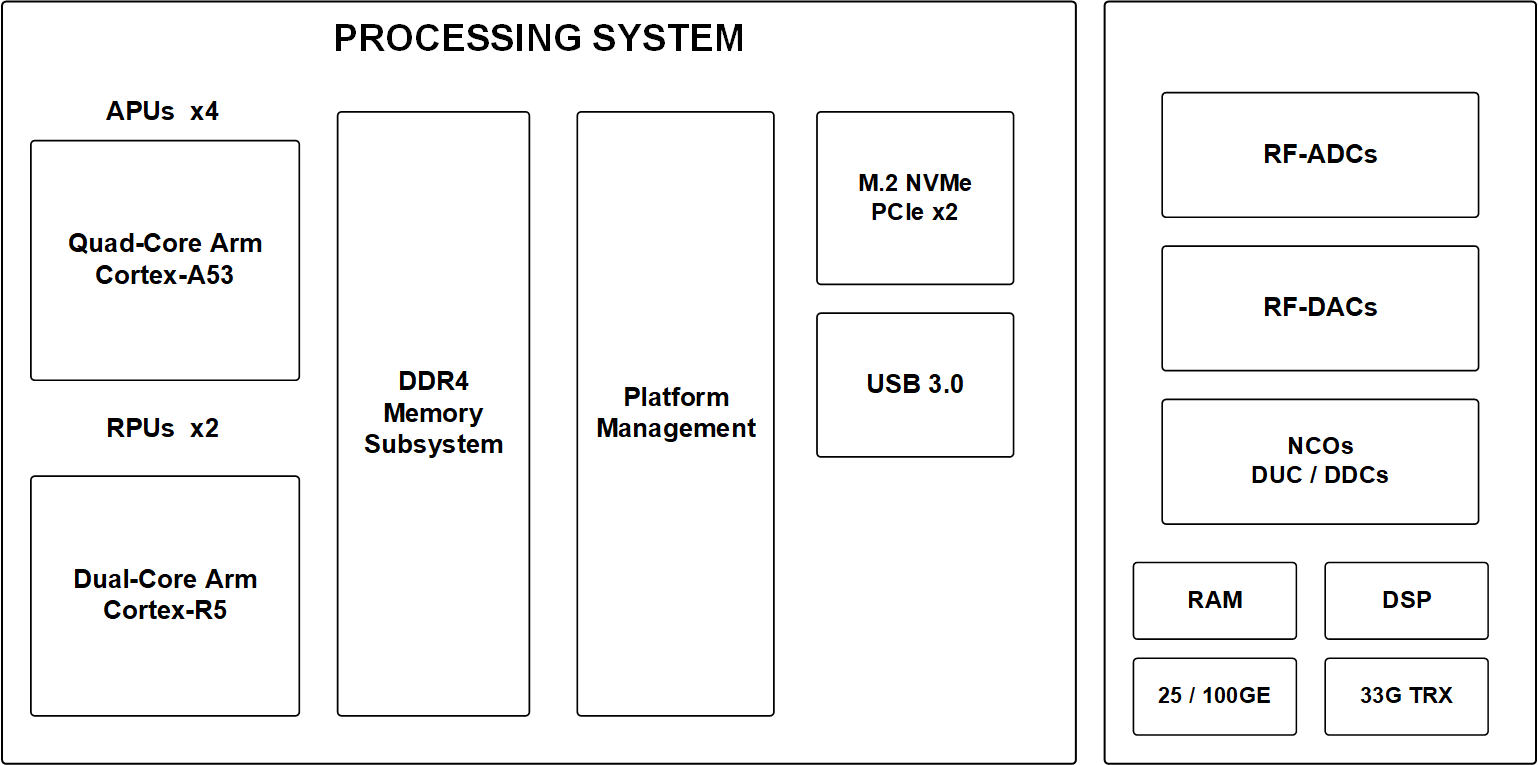
Figure 1.2.1-RFSOM System Block Diagram
1.3 Product Features
Maximize I/O channel density
Supports 8 channels of 14-bit RF-ADC and 8 channels of 14-bit RF-DAC, providing a comprehensive RF signal chain, maximizing input/output channel density, with high bandwidth, heterogeneous processing capability, and low power consumption. It can synchronize all 8 channels and multiple boards to meet larger system application requirements.
Reduce RF signal chain complexity
Radar and EW systems with multiple channels suffer cost and complexity challenges, because more channels mean more expensive and larger RF signal up/down conversion and signal conditioning. A common solution is direct RF sampling - a more flexible approach than traditional analog frequency conversion and filtering. Direct RF sampling can be implemented in the digital domain, which consumes less power and usually costs less. This means the RF front end can handle a wider bandwidth than traditional analog techniques while consuming less power. As with RFSoC devices, using very high sampling rates in the data converters means that most analog filtering and conditioning can be done close to the antenna, providing a simpler and more flexible front end than in the past. By integrating the ADC and DAC into the device, the need for JESD204B is eliminated - simplifying design complexity and helping to reduce latency.
Heterogeneous processing capability
Systems such as radar and electronic warfare require streaming DSP with FPGA and general-purpose processors for decision-making and control. In the past, these processing requirements were handled by separate modules. Now, with the AXW48, both functions can be integrated into one module by leveraging RFSoC technology. This is especially applicable to the growing demands of today's smart radar/electronic warfare technology. In addition, simplified integration with RF sampling devices eliminates the complexity of the JESD204B high-speed serial interface. This means basic functions such as inter-device communication consume fewer programmable logic elements, leaving more computing resources available for application-specific IP than in the past.
1.4 Application Scenarios
Communication application scenarios
5G and LTE wireless technology: With the Zynq RFSoC, wireless infrastructure manufacturers can achieve significant board area and power consumption reduction, which is crucial to the development of MIMO technology in the later stage.
Satellite communication: Designers can build high-speed multifunctional instruments for signal generation and signal analysis by using direct RF sampling, highly flexible, reconfigurable logic, and software programmability in the Zynq UltraScale+ RFSoC.
Radar application scenarios
Radar signal processing and data links: With 8-channel ADC and 8-channel DAC, it can meet larger application requirements and achieve low-latency transmission and reception in early warning scenarios, obtaining the best response time.
Test and measurement application scenarios
Designers can build high-speed multifunctional instruments for signal generation and signal analysis by utilizing RF sampling, highly flexible, reconfigurable logic, and software programmability in the Zynq UltraScale+ RFSoC.
Maximize I/O channel density
Supports 8 channels of 14-bit RF-ADC and 8 channels of 14-bit RF-DAC, providing a comprehensive RF signal chain, maximizing input/output channel density, with high bandwidth, heterogeneous processing capability, and low power consumption. It can synchronize all 8 channels and multiple boards to meet larger system application requirements.
Reduce RF signal chain complexity
Radar and EW systems with multiple channels suffer cost and complexity challenges, because more channels mean more expensive and larger RF signal up/down conversion and signal conditioning. A common solution is direct RF sampling - a more flexible approach than traditional analog frequency conversion and filtering. Direct RF sampling can be implemented in the digital domain, which consumes less power and usually costs less. This means the RF front end can handle a wider bandwidth than traditional analog techniques while consuming less power. As with RFSoC devices, using very high sampling rates in the data converters means that most analog filtering and conditioning can be done close to the antenna, providing a simpler and more flexible front end than in the past. By integrating the ADC and DAC into the device, the need for JESD204B is eliminated - simplifying design complexity and helping to reduce latency.
Heterogeneous processing capability
Systems such as radar and electronic warfare require streaming DSP with FPGA and general-purpose processors for decision-making and control. In the past, these processing requirements were handled by separate modules. Now, with the AXW48, both functions can be integrated into one module by leveraging RFSoC technology. This is especially applicable to the growing demands of today's smart radar/electronic warfare technology. In addition, simplified integration with RF sampling devices eliminates the complexity of the JESD204B high-speed serial interface. This means basic functions such as inter-device communication consume fewer programmable logic elements, leaving more computing resources available for application-specific IP than in the past.
Communication application scenarios
5G and LTE wireless technology: With the Zynq RFSoC, wireless infrastructure manufacturers can achieve significant board area and power consumption reduction, which is crucial to the development of MIMO technology in the later stage.
Satellite communication: Designers can build high-speed multifunctional instruments for signal generation and signal analysis by using direct RF sampling, highly flexible, reconfigurable logic, and software programmability in the Zynq UltraScale+ RFSoC.
Radar application scenarios
Radar signal processing and data links: With 8-channel ADC and 8-channel DAC, it can meet larger application requirements and achieve low-latency transmission and reception in early warning scenarios, obtaining the best response time.
Test and measurement application scenarios
Designers can build high-speed multifunctional instruments for signal generation and signal analysis by utilizing RF sampling, highly flexible, reconfigurable logic, and software programmability in the Zynq UltraScale+ RFSoC.
Part 2: Platform Hardware Introduction
2.1 Hardware Block Diagram
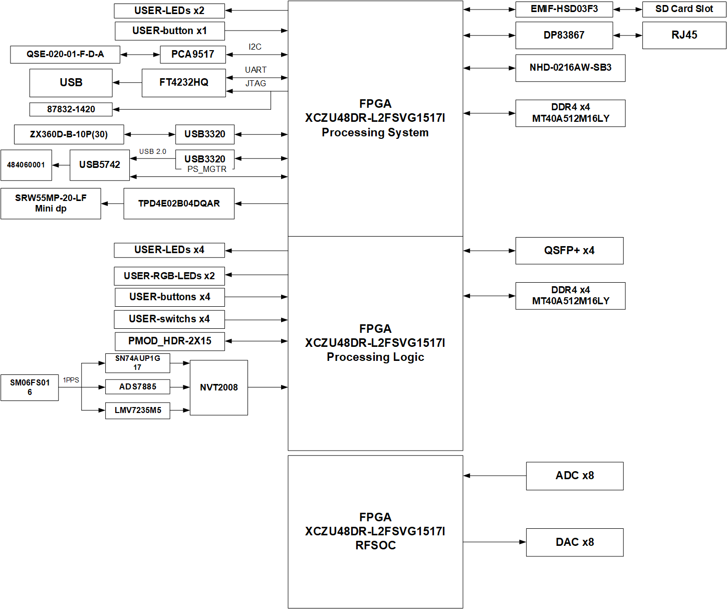
Figure 2.1.1-AXW48 Board Block Diagram
2.2 Key Specifications
| Technical Specifications | |
| FPGA Chip | Zynq UltraScale+ XCZU48DR-L2FSVG1517I |
| RF Interface | 1. x8 ADC (14-bit, 5 GSPS) ports1. x8 DAC (14-bit, 9.85 GSPS) ports |
| 100G Optical Ports | 4 |
| Interface Rate | Display Port*1 |
| Memory | PS 4x DDR4 (4GB, 64bit) PL 4x DDR4 (4GB, 64bit) |
| Board Power Supply | Powered via a 12 V power supply interface |
| PS-Side Interfaces | - 2x USB 3.0 Port- 1x 10/100/1000 Ethernet RGMII (RJ45) port- 1x Micro SD Card- 1x Display Port- 1x OLED |
| PL-Side Interfaces | - 1x SYZYGY connector- 1x PMOD connector- 8 ADC ports (14-bit, 5 GSPS)- 8 DAC ports (14-bit, 9.85 GSPS) |
| Dimensions | 260.0604 mm x 209.9996 mm |
| Power Consumption | 60 W (measured value depending on application) |
| Ambient Temperature Requirement | -40°C to 70°C (operating) |
| Reference Designs | |
| - Host software for configuring ADC/DAC related registers- High-speed ADC/DAC loopback test project- Schematics (in .pdf format)- DDR4 reference design- FPGA pin layout | |
2.3 Functions and Locations
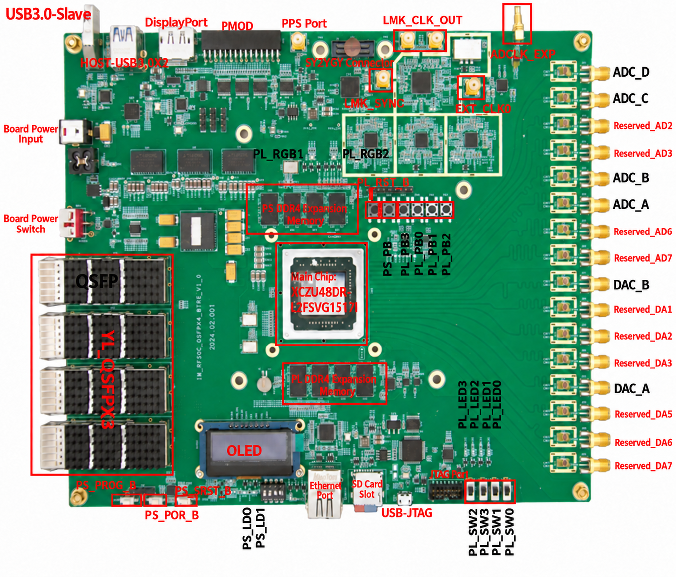
Figure 2.3.1-AXW48 Board Function Diagram
2.4 Boot Mode
The board has 2 boot modes: JTAG mode and SD card mode. The boot mode of the XCZU48DR can be configured through the DIP switch SW2.
The main chip of this board, the XCZU48DR (reference designator U32), is an RFSoC FPGA. The boot mode is determined by the high/low states of the 4 pins PS_MODE0, PS_MODE1, PS_MODE2, and PS_MODE3. The board selects the device configuration mode through the 4-position switch SW2.
| BOOT Mode | Mode pin [3:0] | SW[4:1] |
| JTAG | 0000 | OFF, OFF, OFF, OFF |
| SD | 0011 | OFF, OFF, ON, ON |
Table 2.4.1-SW2 Boot Mode Configuration
2.5 DDR4 SDRAM
The board is equipped with 8 Micron 1 GB DDR4 chips. Four DDR4 chips are mounted on the PS side, forming a 64-bit data bus bandwidth, with model MT40A512M16LY-062E IT:E. Four DDR4 chips are mounted on the PL side, forming a 64-bit data bus bandwidth, with model MT40A512M16LY-062E IT:E. The PS-side DDR4 SDRAM can reach a maximum data rate of 2400 Mb/s, and the 4-chip DDR4 memory system is directly connected to the memory interface of PS BANK504. The PL-side DDR4 SDRAM has a maximum data rate of 2666 Mb/s, and the 4 DDR4 chips are connected to the interfaces of FPGA BANKs 67, 68, and 69. The detailed configurations of the PS-side and PL-side DDR4 SDRAM are shown in the following table:
| Position | Reference | Part Number | Capacity | Factory |
| PS | U30, U36, U26, U23 | MT40A512M16LY-062E IT:E | 512x16bit | Micron |
| PL | U40, U41, U42, U43 | MT40A512M16LY-062E IT:E | 512x16bit | Micron |
Table 2.5.1-DDR4 Configuration
The hardware connection of the PS-side DDR4 is shown in the following figure:
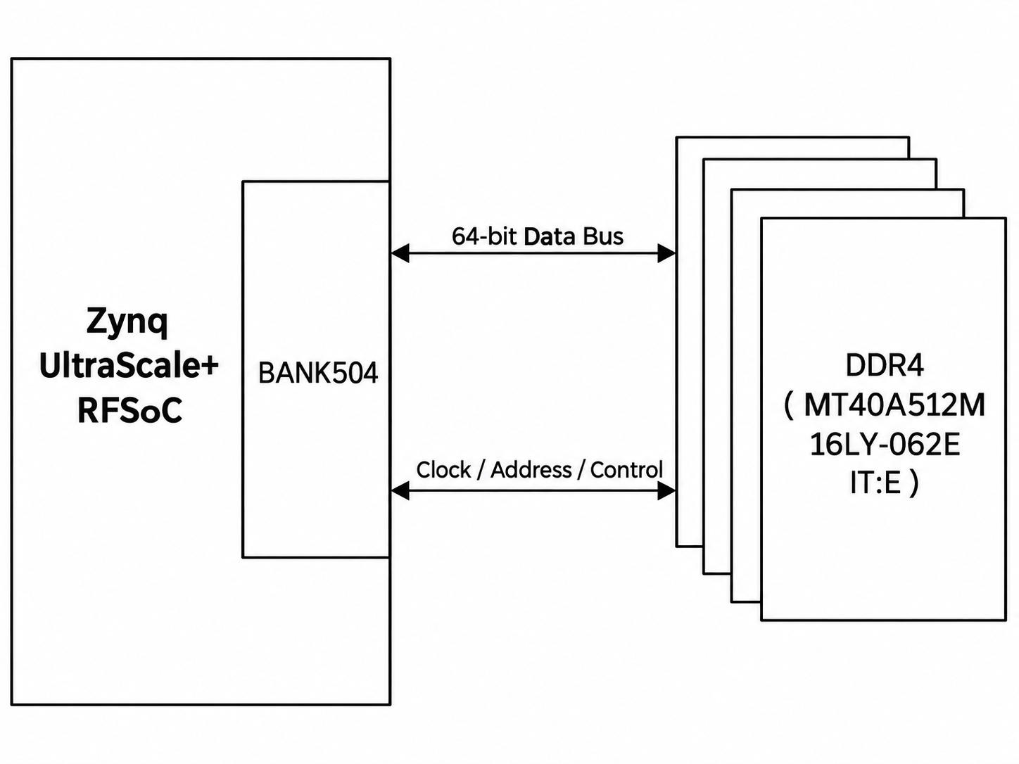
Figure 2.5.1-PS DDR4 Connection Diagram
The hardware connection of the PL-side DDR4 is shown in the following figure:
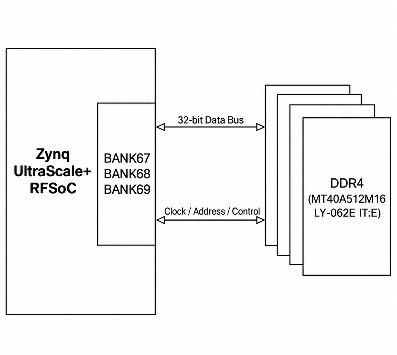
Figure 2.5.2-PL DDR4 Connection Diagram
2.6 Micro SD Card Socket
The AXW48 includes a Micro SD card interface to provide users with access to the SD card storage, which is used to store the BOOT program, the Linux operating system kernel, the file system, and other user data files. The SD card IO signals are connected to the MIO signals of PS BANK501. The connection between the PS and the SD card connector is shown in the following figure:
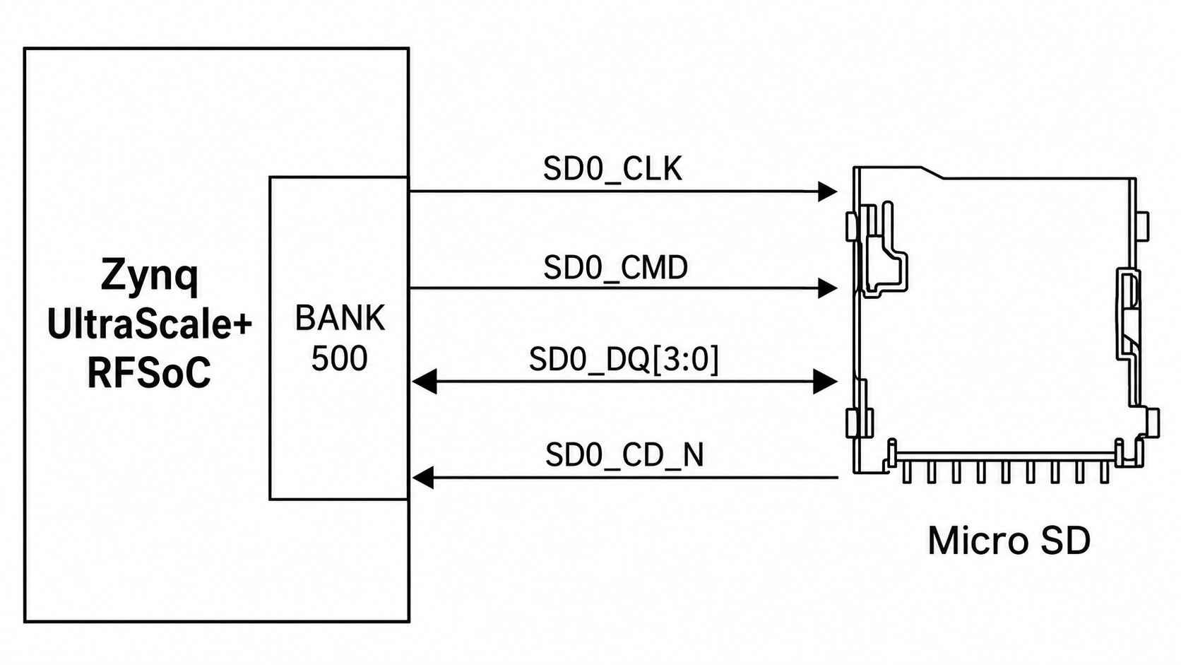
Figure 2.6.1-SD Card Connection Diagram
| Signal Name | Pin Name | Pin Number | Remarks |
| MIO25_SDO_WP_N | PS_MIO25_W29 | W29 | Detects whether the SD card is in write-protect state |
| MIO24_SDO_CD_N | PS_MIO24_Y29 | Y29 | SD card detect signal |
| MIO22_SDO_CLK | PS_MIO22_Y28 | Y28 | SD clock signal |
| MIO21_SDO_CMD | PS_MIO21_V29 | V29 | SD command signal |
| MIO16_SDO_DQ3 | PS_MIO16_R29 | R29 | SD data Bit3 |
| MIO15_SDO_DQ2 | PS_MIO15_U28 | U28 | SD data Bit2 |
| MIO14_SDO_DQ1 | PS_MIO14_P29 | P29 | SD data Bit1 |
| MIO13_SDO_DQ0 | PS_MIO13_R28 | R28 | SD data Bit0 |
Table 2.6.1-SD Card Pin Assignment
2.7 USB3.0 Interface
The PS side of the board supports USB3.0 with HOST and SLAVE working modes, and data transfer rates up to 5.0 Gb/s. USB3.0 is connected to the external Type-A interface, and USB2.0 is connected to the external USB3320C chip through the ULPI interface, realizing high-speed USB3.0 and USB2.0 data communication. The USB3.0 connection diagram is shown below:
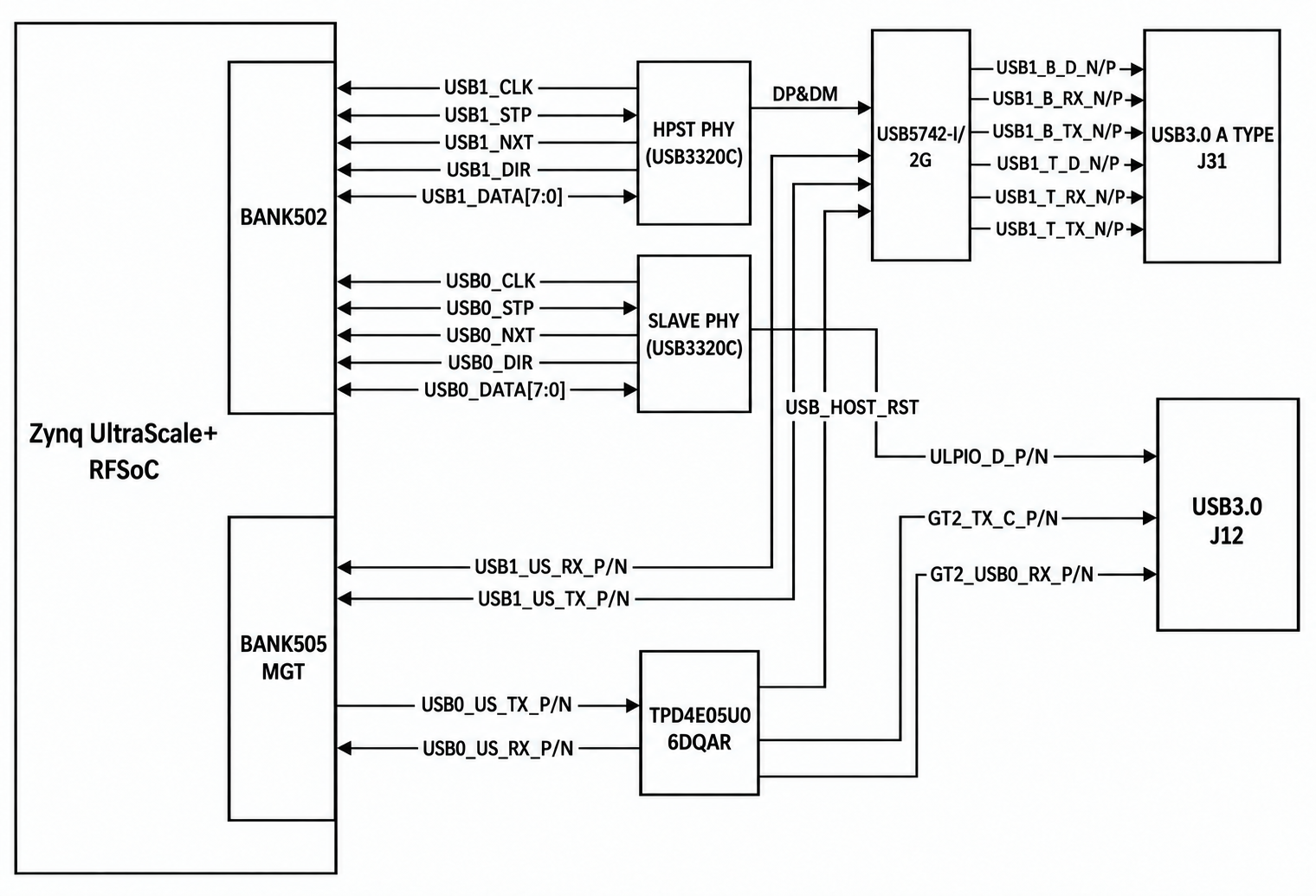
Figure 2.7.1-USB3.0 Interface Diagram
| Signal Name | Pin Name | ZYNQ Pin Number | Remarks |
| MIO77_USB_VBUS_DET | PS_MIO77_L29 | L29 | USB2.0 (1) status signal |
| MIO76_USB_RESET_B | PS_MIO76_M29 | M29 | USB2.0 (1) reset signal |
| MIO75_USB1_D7 | PS_MIO75_N28 | N28 | USB2.0 (1) data Bit7 |
| MIO74_USB1_D6 | PS_MIO74_M28 | M28 | USB2.0 (1) data Bit6 |
| MIO73_USB1_D5 | PS_MIO73_K29 | K29 | USB2.0 (1) data Bit5 |
| MIO72_USB1_D4 | PS_MIO72_J29 | J29 | USB2.0 (1) data Bit4 |
| MIO71_USB1_D3 | PS_MIO71_H28 | H28 | USB2.0 (1) data Bit3 |
| MIO70_USB1_STP | PS_MIO70_K28 | K28 | USB2.0 (1) stop signal |
| MIO69_USB1_D1 | PS_MIO69_M27 | M27 | USB2.0 (1) data Bit1 |
| MIO68_USB1_D0 | PS_MIO68_H29 | H29 | USB2.0 (1) data Bit0 |
| MIO67_USB1_NXT | PS_MIO67_J28 | J28 | USB2.0 (1) next data signal |
| MIO66_USB1_D2 | PS_MIO66_N27 | N27 | USB2.0 (1) data Bit2 |
| MIO65_USB1_DIR | PS_MIO65_L27 | L27 | USB2.0 (1) data direction signal |
| MIO64_USB1_CLK | PS_MIO64_K27 | K27 | USB2.0 (1) clock signal |
| MIO63_USB0_D7 | PS_MIO63_G29 | G29 | USB2.0 (0) data Bit7 |
| MIO62_USB0_D6 | PS_MIO62_K26 | K26 | USB2.0 (0) data Bit6 |
| MIO61_USB0_D5 | PS_MIO61_G28 | G28 | USB2.0 (0) data Bit5 |
| MIO60_USB0_D4 | PS_MIO60_J26 | J26 | USB2.0 (0) data Bit4 |
| MIO59_USB0_D3 | PS_MIO59_H27 | H27 | USB2.0 (0) data Bit3 |
| MIO58_USB0_STP | PS_MIO58_H26 | H26 | USB2.0 (0) stop signal |
| MIO57_USB0_D1 | PS_MIO57_H25 | H25 | USB2.0 (0) data Bit1 |
| MIO56_USB0_D0 | PS_MIO56_L26 | L26 | USB2.0 (0) data Bit0 |
| MIO55_USB0_NXT | PS_MIO55_J25 | J25 | USB2.0 (0) next data signal |
| MIO54_USB0_D2 | PS_MIO54_M26 | M26 | USB2.0 (0) data Bit2 |
| MIO53_USB0_DIR | PS_MIO53_L25 | L25 | USB2.0 (0) data direction signal |
| MIO52_USB0_CLK | PS_MIO52_N26 | N26 | USB2.0 (0) clock signal |
| USB0_US_TX_P | PS_MGTRTXP2_505_AF36 | AF36 | USB3.0 (0) transmit positive |
| USB0_US_TX_N | PS_MGTRTXN2_505_AF37 | AF37 | USB3.0 (0) transmit negative |
| USB0_US_TX_P | PS_MGTRRXP2_505_AE38 | AE38 | USB3.0 (0) receive positive |
| USB0_US_RX_N | PS_MGTRRXN2_505_AE39 | AE39 | USB3.0 (0) receive negative |
| USB1_US_TX_P | PS_MGTRTXP3_505_AD36 | AD36 | USB3.0 (1) transmit positive |
| USB1_US_TX_N | PS_MGTRTXN3_505_AD37 | AD37 | USB3.0 (1) transmit negative |
| USB1_US_RX_P | PS_MGTRRXP3_505_AC38 | AC38 | USB3.0 (1) receive positive |
| USB1_US_RX_N | PS_MGTRRXN3_505_AC39 | AC39 | USB3.0 (1) receive negative |
Table 2.7.1-USB3.0 Interface Pin Assignment
2.8 Ethernet
The AXW48 has one gigabit Ethernet interface on the PS side. The Ethernet chip adopts TI's (Texas Instruments) DP83867IRRGZ chip to provide network communication services for users. The Ethernet PHY chip on the PS side is connected to the MIO of PS BANK501 on the ZYNQ. The DP83867IRRGZ chip supports 10/100/1000 Mbps network transfer rates and communicates data with the MAC layer of the ZYNQ system through the RGMII interface. The connection diagram of the gigabit Ethernet PHY chip is shown in the following figure:
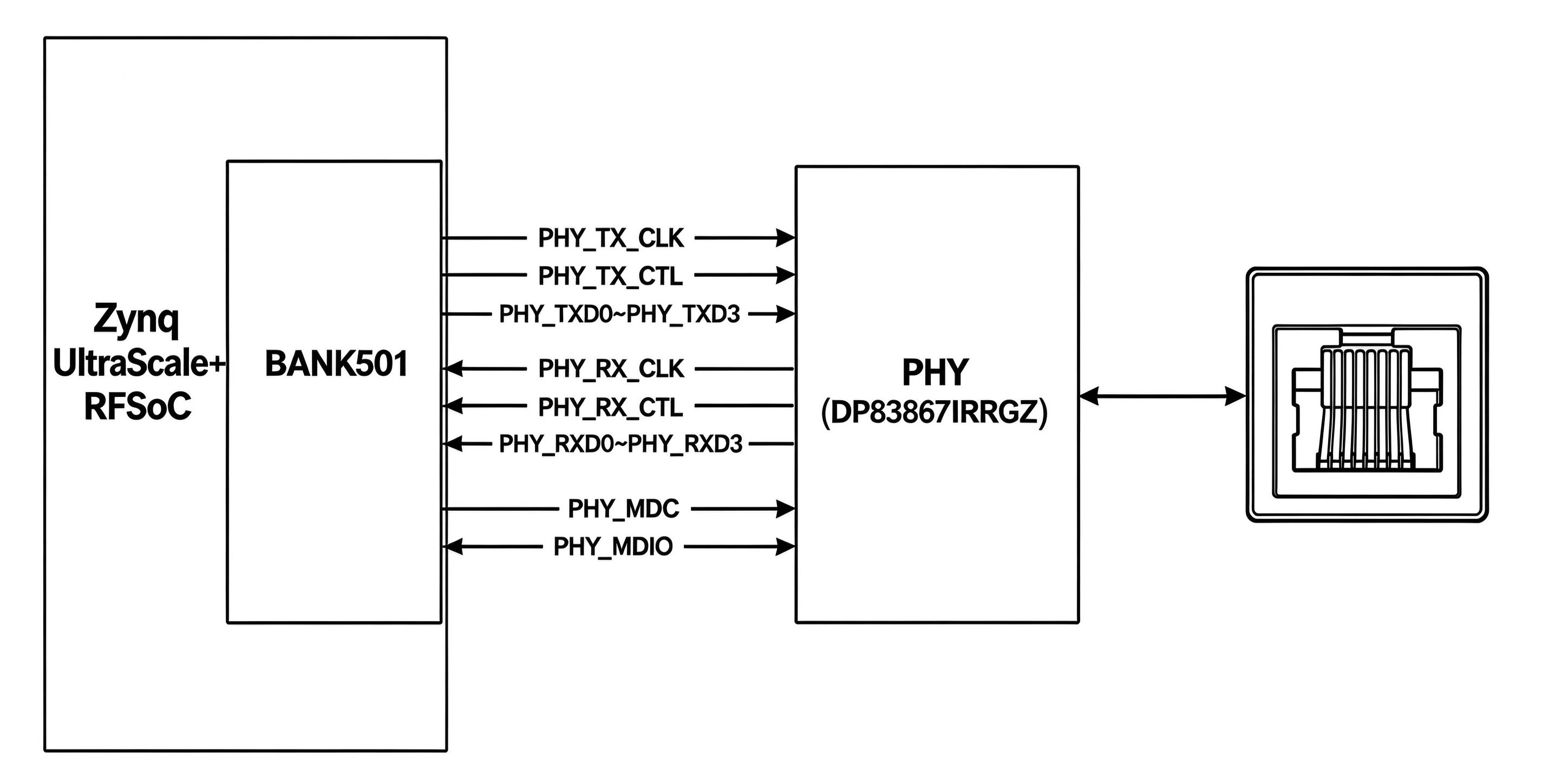
Figure 2.8.1-PS Ethernet Connection Diagram
| Signal Name | Pin Name | Pin Number | PHY Chip | |
| Pin Number | Pin Name | |||
| MIO51_GEM1_MDIO | PS_MIO51_E29 | E29 | 17 | MDIO |
| MIO50_GEM1_MDC | PS_MIO50_F29 | F29 | 16 | MDC |
| MIO38_GEM1_TX_CLK | PS_MIO38_E27 | E27 | 29 | TX_CLK |
| MIO43_GEM1_TX_CTL | PS_MIO43_D28 | D28 | 37 | TX_CTRL |
| MIO42_GEM1_TX_D3 | PS_MIO42_E28 | E28 | 25 | TXD3 |
| MIO41_GEM1_TX_D2 | PS_MIO41_C28 | C28 | 26 | TXD2 |
| MIO40_GEM1_TX_D1 | PS_MIO40_D26 | D26 | 27 | TXD1 |
| MIO39_GEM1_TX_D0 | PS_MIO39_B28 | B28 | 28 | TXD0 |
| MIO44_GEM1_RX_CLK | PS_MIO44_F27 | F27 | 32 | RXCLK |
| MIO49_GEM1_RX_CTRL | PS_MIO49_B29 | B29 | 38 | RX_CTRL |
| MIO48_GEM1_RX_D3 | PS_MIO48_D29 | D29 | 36 | RXD3 |
| MIO47_GEM1_RX_D2 | PS_MIO47_C29 | C29 | 35 | RXD2 |
| MIO46_GEM1_RX_D1 | PS_MIO46_A29 | A29 | 34 | RXD1 |
| MIO45_GEM1_RX_D0 | PS_MIO45_G27 | G27 | 33 | RXD0 |
Table 2.8.1-PHY Pin Assignment Connected to the PS Side of the XCZU48DR RFSoC
2.9 Optical Ports
The AXW48 has 4 QSFP interfaces. The 4 optical fiber interfaces are connected to the GTY transceivers on ZYNQ BANKs 128 to 131, respectively. CLK1 of BANK129 and BANK131 is provided by a differential crystal oscillator. CLK0 of BANKs 128, 129, 130, and 131 is provided by the Si5395B-A-GM, supplying a 156.25 MHz clock. The QSFP interface connection diagram is shown in the following figure:
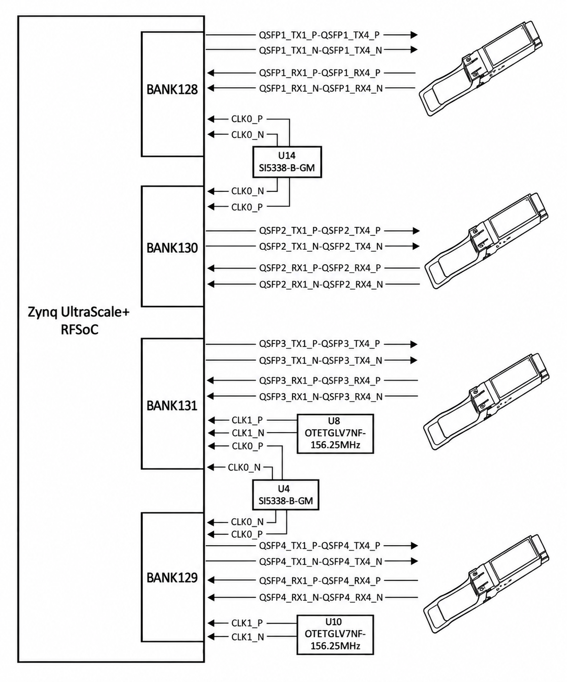
Figure 2.9.1-Optical Fiber Design Diagram
| Signal Name | ZYNQ Pin Name | ZYNQ Pin Number |
| QSFP1_TX1_P | MGTYTXP0_128_Y35 | Y35 |
| QSFP1_TX1_N | MGTYTXN0_128_Y36 | Y36 |
| QSFP1_RX1_P | MGTYRXP0_128_AA38 | AA38 |
| QSFP1_RX1_N | MGTYRXN0_128_AA39 | AA39 |
| QSFP1_TX2_P | MGTYTXP1_128_V35 | V35 |
| QSFP1_TX2_N | MGTYTXN1_128_V36 | V36 |
| QSFP1_RX2_P | MGTYRXP1_128_W38 | W38 |
| QSFP1_RX2_N | MGTYRXN1_128_W39 | W39 |
| QSFP1_TX3_P | MGTYTXP2_128_T35 | T35 |
| QSFP1_TX3_N | MGTYTXN2_128_T36 | T36 |
| QSFP1_RX3_P | MGTYRXP2_128_U38 | U38 |
| QSFP1_RX3_N | MGTYRXN2_128_U39 | U39 |
| QSFP1_TX4_P | MGTYTXP3_128_R33 | R33 |
| QSFP1_TX4_N | MGTYTXN3_128_R34 | R34 |
| QSFP1_RX4_P | MGTYRXP3_128_R38 | R38 |
| QSFP1_RX4_N | MGTYRXN3_128_R39 | R39 |
| QSFP2_TX1_P | MGTYTXP0_130_H31 | H31 |
| QSFP2_TX1_N | MGTYTXN0_130_H32 | H32 |
| QSFP2_RX1_P | MGTYRXP0_130_J38 | J38 |
| QSFP2_RX1_N | MGTYRXN0_130_J39 | J39 |
| QSFP2_TX2_P | MGTYTXP1_130_G33 | G33 |
| QSFP2_TX2_N | MGTYTXN1_130_G34 | G34 |
| QSFP2_RX2_P | MGTYRXP1_130_H36 | H36 |
| QSFP2_RX2_N | MGTYRXP1_130_H37 | H37 |
| QSFP2_TX3_P | MGTYTXP2_130_F31 | F31 |
| QSFP2_TX3_N | MGTYTXP2_130_F32 | F32 |
| QSFP2_RX3_P | MGTYRXP2_130_G38 | G38 |
| QSFP2_RX3_N | MGTYRXP2_130_G39 | G39 |
| QSFP2_TX4_P | MGTYTXP3_130_E33 | E33 |
| QSFP2_TX4_N | MGTYTXP3_130_E34 | E34 |
| QSFP2_RX4_P | MGTYRXP3_130_F36 | F36 |
| QSFP2_RX4_N | MGTYRXP3_130_F37 | F37 |
| QSFP3_TX1_P | MGTYTXP0_131_D31 | D31 |
| QSFP3_TX1_N | MGTYTXP0_131_D32 | D32 |
| QSFP3_RX1_P | MGTYRXP0_131_E38 | E38 |
| QSFP3_RX1_N | MGTYRXP0_131_E39 | E39 |
| QSFP3_TX2_P | MGTYTXP1_131_C33 | C33 |
| QSFP3_TX2_N | MGTYTXP1_131_C34 | C34 |
| QSFP3_RX2_P | MGTYRXP1_131_D36 | D36 |
| QSFP3_RX2_N | MGTYRXP1_131_D37 | D37 |
| QSFP3_TX3_P | MGTYTXP2_131_B31 | B31 |
| QSFP3_TX3_N | MGTYTXP2_131_B32 | B32 |
| QSFP3_RX3_P | MGTYRXP2_131_C38 | C38 |
| QSFP3_RX3_N | MGTYRXP2_131_C39 | C39 |
| QSFP3_TX4_P | MGTYTXP3_131_A33 | A33 |
| QSFP3_TX4_N | MGTYTXP3_131_A34 | A34 |
| QSFP3_RX4_P | MGTYRXP3_131_B36 | B36 |
| QSFP3_RX4_N | MGTYRXP3_131_B37 | B37 |
| QSFP4_TX1_P | MGTYTXP0_129_P35 | P35 |
| QSFP4_TX1_N | MGTYTXP0_129_P36 | P36 |
| QSFP4_RX1_P | MGTYRXP0_129_N38 | N38 |
| QSFP4_RX1_N | MGTYRXP0_129_N39 | N39 |
| QSFP4_TX2_P | MGTYTXP1_129_N33 | N33 |
| QSFP4_TX2_N | MGTYTXP1_129_N34 | N34 |
| QSFP4_RX2_P | MGTYRXP1_129_M36 | M36 |
| QSFP4_RX2_N | MGTYRXP1_129_M37 | M37 |
| QSFP4_TX3_P | MGTYTXP2_129_L33 | L33 |
| QSFP4_TX3_N | MGTYTXP2_129_L34 | L34 |
| QSFP4_RX3_P | MGTYRXP2_129_L38 | L38 |
| QSFP4_RX3_N | MGTYRXP2_129_L39 | L39 |
| QSFP4_TX4_P | MGTYTXP3_129_J33 | J33 |
| QSFP4_TX4_N | MGTYTXP3_129_J34 | J34 |
| QSFP4_RX4_P | MGTYRXP3_129_K36 | K36 |
| QSFP4_RX4_N | MGTYRXP3_129_K37 | K37 |
Table 2.9.1-QSFP1 to QSFP4 Interface Pin Assignment
| Signal Name | ZYNQ Pin Name | ZYNQ Pin Number | Remarks |
| QSFP1_CLK_P | MGTREFCLK1P_129_V31 | V31 | 156.25 MHz differential output |
| QSFP1_CLK_N | MGTREFCLK1P_129_V32 | V32 | 156.25 MHz differential output |
| QSFP2_CLK_P | MGTREFCLK1P_131_M31 | M31 | 156.25 MHz differential output |
| QSFP2_CLK_N | MGTREFCLK1P_131_M32 | M32 | 156.25 MHz differential output |
| GTY_129_REF_CLK_QSFP_P | MGTREFCLK0P_129_W33 | W33 | Si5395B-A-GM OUT3 output 156.25 MHz |
| GTY_129_REF_CLK_QSFP_N | MGTREFCLK0N_129_W34 | T35 | Si5395B-A-GM OUT3 output 156.25 MHz |
| GTY_130_REF_CLK_QSFP_P | MGTREFCLK0P_130_U33 | U33 | Si5395B-A-GM OUT7 output 156.25 MHz |
| GTY_130_REF_CLK_QSFP_N | MGTREFCLK0N_130_U34 | U34 | Si5395B-A-GM OUT7 output 156.25 MHz |
| GTY_131_REF_CLK_QSFP_P | MGTREFCLK0P_131_P31 | P31 | Si5395B-A-GM OUT5 output 156.25 MHz |
| GTY_131_REF_CLK_QSFP_N | MGTREFCLK0N_131_P32 | P32 | Si5395B-A-GM OUT5 output 156.25 MHz |
Table 2.9.2-BANK129 and BANK130 Reference Clock Assignment
Low-speed control IO handling:
| QSFP Low-Speed IO Signal Name | Remarks |
| MODPRSL | Pulled up to 3.3 V |
| INTL | Pulled up to 3.3 V |
Table 2.9.3-Optical Fiber Low-Speed IO Signal Handling
2.10 RF
The product supports 8 channels of 14-bit ADC input at 5 GSPS and 8 channels of 14-bit DAC output at 9.85 GSPS. The RF connector is the SMA-KHDC16, with single-ended signal input and output. Differential-to-single-ended conversion is performed through balun devices to complete data transmission and reception, and the VCM signals are also routed to the TP, making it convenient for users to adjust the common-mode voltage.
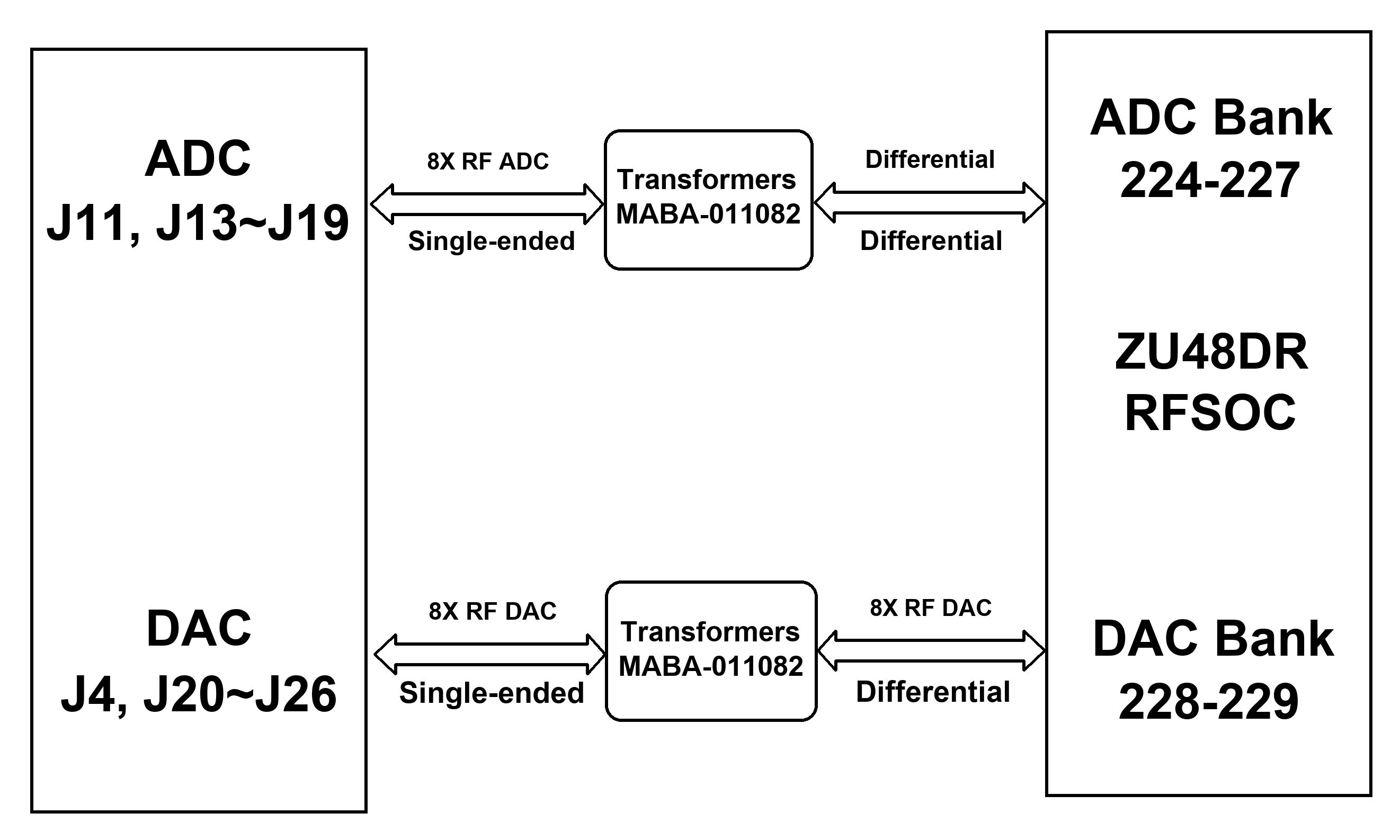
Figure 2.10.1-ADC & DAC Connection Diagram
| Signal Name | ZYNQ Pin Name | ZYNQ Pin Number |
| RFMC_ADC_00_P | ADC_VIN_I01_P_224_AP2 | AP2 |
| RFMC_ADC_00_N | ADC_VIN_I01_N_224_AP1 | AP1 |
| RFMC_ADC_01_P | ADC_VIN_I23_P_224_AM2 | AM2 |
| RFMC_ADC_01_N | ADC_VIN_I23_N_224_AM1 | AM1 |
| RFMC_ADC_02_P | ADC_VIN_I01_P_225_AK2 | AK2 |
| RFMC_ADC_02_N | ADC_VIN_I01_N_225_AK1 | AK1 |
| RFMC_ADC_03_P | ADC_VIN_I23_P_225_AH2 | AH2 |
| RFMC_ADC_03_N | ADC_VIN_I23_N_225_AH1 | AH1 |
| RFMC_ADC_04_P | ADC_VIN_I01_P_226_AF2 | AF2 |
| RFMC_ADC_04_N | ADC_VIN_I01_N_226_AF1 | AF1 |
| RFMC_ADC_05_P | ADC_VIN_I23_P_226_AD2 | AD2 |
| RFMC_ADC_05_N | ADC_VIN_I23_N_226_AD1 | AD1 |
| RFMC_ADC_06_P | ADC_VIN_I01_P_227_AB2 | AB2 |
| RFMC_ADC_06_N | ADC_VIN_I01_N_227_AB1 | AB1 |
| RFMC_ADC_07_P | ADC_VIN_I23_P_227_Y2 | Y2 |
| RFMC_ADC_07_N | ADC_VIN_I23_N_227_Y1 | Y1 |
| RFMC_DAC_00_P | DAC_VOUT0_P_228_U2 | U2 |
| RFMC_DAC_00_N | DAC_VOUT0_N_228_U1 | U1 |
| RFMC_DAC_01_P | DAC_VOUT1_P_228_R2 | R2 |
| RFMC_DAC_01_N | DAC_VOUT1_N_228_R1 | R1 |
| RFMC_DAC_02_P | DAC_VOUT2_P_228_N2 | N2 |
| RFMC_DAC_02_N | DAC_VOUT2_N_228_N1 | N1 |
| RFMC_DAC_03_P | DAC_VOUT3_P_228_L2 | L2 |
| RFMC_DAC_03_N | DAC_VOUT3_N_228_L1 | L1 |
| RFMC_DAC_04_P | DAC_VOUT0_P_229_J2 | J2 |
| RFMC_DAC_04_N | DAC_VOUT0_N_229_J1 | J1 |
| RFMC_DAC_05_P | DAC_VOUT1_P_229_G2 | G2 |
| RFMC_DAC_05_N | DAC_VOUT1_N_229_G1 | G1 |
| RFMC_DAC_06_P | DAC_VOUT2_P_229_E2 | E2 |
| RFMC_DAC_06_N | DAC_VOUT2_N_229_E1 | E1 |
| RFMC_DAC_07_P | DAC_VOUT3_P_229_C2 | C2 |
| RFMC_DAC_07_N | DAC_VOUT3_N_229_C1 | C1 |
Table 2.10.1-ADC and DAC Pin Assignment
2.11 Expansion Interfaces
The AXW48 board expands 4 LED lights on the PL side.
| Signal Name | ZYNQ Pin Name | Pin Number |
| PL_USER_LED3 | IO_L6N_T0U_N11_AD6N_65_AU10 | AU10 |
| PL_USER_LED2 | IO_L4N_T0U_N7_DBC_AD7N_65_AT11 | AT11 |
| PL_USER_LED1 | IO_L1N_T0L_N1_DBC_65_AW10 | AW10 |
| PL_USER_LED0 | IO_L8N_T1L_N3_AD5N_65_AR11 | AR11 |
Table 2.11.1-PL Expansion Interface Pin Assignment
The AXW48 board expands 4 push buttons on the PL side.
| Signal Name | ZYNQ Pin Name | Pin Number |
| PL_USER_PB3 | IO_L4P_T0U_N6_DBC_AD7P_SMBALERT_65_AT12 | AT12 |
| PL_USER_PB2 | IO_L5P_T0U_N8_AD14P_65_AW9 | AW9 |
| PL_USER_PB1 | IO_L1P_T0L_N0_DBC_65_AV10 | AV10 |
| PL_USER_PB0 | IO_L2N_T0L_N3_65_AV12 | AV12 |
Table 2.11.2-PL Push Button Expansion Pin Assignment
The AXW48 board has 2 LED lights on the PS side.
| Signal Name | ZYNQ Pin Name | Pin Number |
| PS_LED1 | PS_MIO17_T29 | AT12 |
| PS_LED0 | PS_MIO20_V28 | AW9 |
Table 2.11.3-PS Expansion LED Pin Assignment
The AXW48 board expands an RGB light set on the PL side.
| Signal Name | ZYNQ Pin Name | Pin Number |
| PL_LEDRGB0_B | IO_L16P_T2U_N6_QBC_AD3P_65_AN8 | AN8 |
| PL_LEDRGB0_R | IO_L15P_T2L_N4_AD11P_65_AM8 | AM8 |
| PL_LEDRGB0_G | IO_L15N_T2L_N5_AD11N_65_AM7 | AM7 |
| PL_LEDRGB1_B | IO_L6P_T0U_N10_AD6P_65_AT10 | AT10 |
| PL_LEDRGB1_R | IO_L8P_T1L_N2_AD5P_65_AR12 | AR12 |
| PL_LEDRGB1_G | IO_L13P_T2L_N0_GC_QBC_65_AP8 | AP8 |
Table 2.11.4-PL RGB Expansion Pin Assignment
The AXW48 board expands 4 switches on the PL side.
| Signal Name | ZYNQ Pin Name | Pin Number |
| PL_USER_SW3 | IO_L3P_T0L_N4_AD15P_65_AV11 | AV11 |
| PL_USER_SW2 | IO_L3N_T0L_N5_AD15N_65_AW11 | AW11 |
| PL_USER_SW1 | IO_L2P_T0L_N2_65_AU12 | AU12 |
| PL_USER_SW0 | IO_L10N_T1U_N7_QBC_AD4N_65_AN13 | AN13 |
Table 2.11.5-PL Switch Expansion Pin Assignment
The AXW48 board expands 1 push button on the PS side.
| Signal Name | ZYNQ Pin Name | Pin Number |
| PS_BTN | PS_MIO23_U29 | AV11 |
Table 2.11.6-PS Push Button Expansion Pin Assignment
2.12 PMOD
The AXW48 board includes a 30-pin PMOD port. The PMOD port routes 24 differential FPGA signals to a simple and low-cost 100 mil DIP connector. Users can connect the signals to other custom boards. Among the 30 connector pins available on the PMOD port, 4 are connected to ground, 4 are connected to VDD, and 22 are connected to FPGA signals.
| Signal Name | ZYNQ Pin Name | Pin Number | J29 Pin |
| PMOD0_7 | IO_L14N_T2L_N3_GC_64_AK16 | AK16 | 27 |
| PMOD0_6 | IO_L16N_T2U_N7_QBC_AD3N_64_AH17 | AH17 | 28 |
| PMOD0_5 | IO_L18P_T2U_N10_AD2P_64_AF17 | AF17 | 29 |
| PMOD0_4 | IO_T2U_N12_64_AF15 | AF15 | 30 |
| PMOD0_3 | IO_L14P_T2L_N2_GC_64_AK17 | AK17 | 4 |
| PMOD0_2 | IO_L15P_T2L_N4_AD11P_64_AJ16 | AJ16 | 3 |
| PMOD0_1 | IO_L16P_T2U_N6_QBC_AD3P_64_AG17 | AG17 | 2 |
| PMOD0_0 | IO_L18N_T2U_N11_AD2N_64_AF16 | AF16 | 1 |
| PMOD1_7 | IO_L6N_T0U_N11_AD6N_64_AU14 | AU14 | 18 |
| PMOD1_6 | IO_L5N_T0U_N9_AD14N_64_AT15 | AT15 | 19 |
| PMOD1_5 | IO_L9P_T1L_N4_AD12P_64_AP14 | AP14 | 20 |
| PMOD1_4 | IO_L6P_T0U_N10_AD6P_64_AU15 | AU15 | 21 |
| PMOD1_3 | IO_L3N_T0L_N5_AD15N_64_AV13 | AV13 | 13 |
| PMOD1_2 | IO_L3P_T0L_N4_AD15P_64_AU13 | AU13 | 12 |
| PMOD1_1 | IO_L7N_T1L_N1_QBC_AD13N_64_AR13 | AR13 | 11 |
| PMOD1_0 | IO_L1N_T0L_N1_DBC_64_AW13 | AW13 | 10 |
| PMOD01_5 | IO_L5P_T0U_N8_AD14P_64_AT16 | AT16 | 22 |
| PMOD01_4 | IO_L4P_T0U_N6_DBC_AD7P_64_AV16 | AV16 | 23 |
| PMOD01_3 | IO_L8N_T1L_N3_AD5N_64_AR16 | AR16 | 24 |
| PMOD01_2 | IO_L1P_T0L_N0_DBC_64_AW14 | AW14 | 9 |
| PMOD01_1 | IO_L2N_T0L_N3_64_AW15 | AW15 | 8 |
| PMOD01_0 | IO_L4N_T0U_N7_DBC_AD7N_64_AW16 | AW16 | 7 |
Table 2.12.1-PMOD Connector Interface Pin Assignment
2.13 SYZYGY
The AXW48 board expands a SYZYGY connector. 28 signal lanes can move data at speeds up to 500 MHz, with differential clocks, an I2C bus, a fixed 5 V/3 A power supply, a fixed 3.3 V/3 A power supply, and a user-programmable 3 A, 1.2 V to 3.3 V power supply.
| Signal Name | ZYNQ Pin Name | Pin Number | Connector Pin |
| SYZYGY_D0_N | IO_L4N_AD8N_84_AU1 | AU1 | 7 |
| SYZYGY_D0_P | IO_L4N_AD8P_84_AU2 | AU2 | 5 |
| SYZYGY_D1_N | IO_L11N_AD9N_87_A6 | A6 | 8 |
| SYZYGY_D1_P | IO_L11P_AD9P_87_A7 | A7 | 6 |
| SYZYGY_D2_N | IO_L3N_AD9N_84_AU2 | AU2 | 11 |
| SYZYGY_D2_P | IO_L3N_AD9P_84_AV2 | AV2 | 9 |
| SYZYGY_D3_N | IO_L5N_HDGC_87_C7 | C7 | 14 |
| SYZYGY_D3_P | IO_L5P_HDGC_87_C8 | C8 | 12 |
| SYZYGY_D4_N | IO_L2N_AD10N_84_AW3 | AW3 | 15 |
| SYZYGY_D4_P | IO_L2P_AD10P_84_AW4 | AW4 | 13 |
| SYZYGY_D5_N | IO_L2N_AD14N_87_E8 | E8 | 16 |
| SYZYGY_D5_P | IO_L2P_AD14P_87_E9 | E9 | 14 |
| SYZYGY_D6_N | IO_L8N_HDGC_AD4N_84_AT6 | AT6 | 19 |
| SYZYGY_D6_P | IO_L8P_HDGC_AD4P_84_AT7 | AT7 | 17 |
| SYZYGY_D7_N | IO_L1N_AD15N_87_E6 | E6 | 20 |
| SYZYGY_D7_P | IO_L1P_AD15P_87_F6 | F6 | 18 |
| SYZYGY_S16 | IO_L7P_HDGC_87_B8 | B8 | 21 |
| SYZYGY_S17 | IO_L11N_AD1N_84_AR6 | AR6 | 22 |
| SYZYGY_S18 | IO_L3N_AD13N_87_D6 | D6 | 23 |
| SYZYGY_S19 | IO_L11P_AD1P_84_AR7 | AR7 | 24 |
| SYZYGY_S20 | IO_L9P_AD11P_87_C6 | C6 | 25 |
| SYZYGY_S21 | IO_L10P_AD2P_84_AU7 | AU7 | 26 |
| SYZYGY_S22 | IO_L10P_AD10P_87_B5 | B5 | 27 |
| SYZYGY_S23 | IO_L10N_AD2N_84_AV7 | AV7 | 28 |
| SYZYGY_S24 | IO_L10N_AD10N_87_A5 | A5 | 29 |
| SYZYGY_S25 | IO_L9P_AD3P_84_AU8 | AU8 | 30 |
| SYZYGY_S26 | IO_L9N_AD11N_87_C5 | C5 | 31 |
| SYZYGY_S27 | IO_L9N_AD3N_84_AV8 | AV8 | 32 |
| SYZYGY_P2C_CLK_N | IO_L5N_HDGC_AD7N_84_AV5 | AV5 | 35 |
| SYZYGY_P2C_CLK_P | IO_L5P_HDGC_AD7P_84_AV6 | AV6 | 33 |
| SYZYGY_C2P_CLK_N | IO_L8N_HDGC_87_B9 | B9 | 36 |
| SYZYGY_C2P_CLK_P | IO_L8P_HDGC_87_B10 | B10 | 34 |
Table 2.13.1-SYZYGY Connector Interface Pin Assignment
2.14 Display Port
The AXW48 board has a mini Display Port interface for driving high-resolution displays. It can drive high-speed serial transceivers up to 6 Gb/s, so no other interface components are required. The DisplayPort interface provides multiple interfaces to process real-time audio/video feeds from the PS or PL, or to store audio/video from the memory frame buffer. It supports two audio/video pipelines simultaneously, providing instant rendering capabilities. If the current drawn from the connector exceeds 2.5 A, the TPD8S009DSMR e-fuse will interrupt the power flow of the Display Port 3.3 V power pin.
| Signal Name | ZYNQ Pin Name | ZYNQ Pin Number |
| DP1_TX_P | PS_MGTRTXP0_505_AK36 | AK36 |
| DP1_TX_N | PS_MGTRTXN0_505_AK37 | AK37 |
| DP0_TX_P | PS_MGTRTXP1_505_AH36 | AH36 |
| DP0_TX_N | PS_MGTRTXN1_505_AH37 | AH37 |
| MIO27_DP_AUX_DATA_OUT | PS_MIO27_C25 | C25 |
| MIO29_DP_AUX_DATA_OE | PS_MIO29_B25 | B25 |
| MIO30_DP_AUX_DATA_IN | PS_MIO30_D25 | D25 |
| MIO28_DP_HPD | PS_MIO28_F25 | F25 |
Table 2.14.1-Display Port Interface Pin Assignment
2.15 OLED
The AXW48 board includes an NHD-0216AW-SB3 16x2 character display, connected to the processing system via the SPI bus. The default PYNQ framework uses this display to show the board status during boot and normal operation. Drivers that allow displaying custom messages are available in the framework.
| Signal Name | ZYNQ Pin Name | Pin Number |
| OLED_SPI_SCLK | PS_MIO6_W26 | W26 |
| OLED_SPI_MOSI | PS_MIO11_P28 | P28 |
| OLED_SPI_MISO | PS_MIO10_V27 | V27 |
| OLED_SPI_CSn | PS_MIO9_R27 | R27 |
Table 2.15.1-OLED Pin Assignment
2.16 Clock Configuration
The AXW48 provides multiple clock options. The core module provides dual crystal oscillator clocks, and the system clock defaults to a 33.33 MHz active crystal oscillator. The X9 crystal at 32.768 kHz drives the internal RTC circuit.
The board uses the Si5395B-A-GM to generate the required clocks, and the LMK04828 clock chip to distribute the clocks required by each module. The main crystal oscillator is a 160 MHz crystal. GTY recovered clocks are supported, enabling multiple modules to be connected in parallel to form larger-scale coherent RF channels.
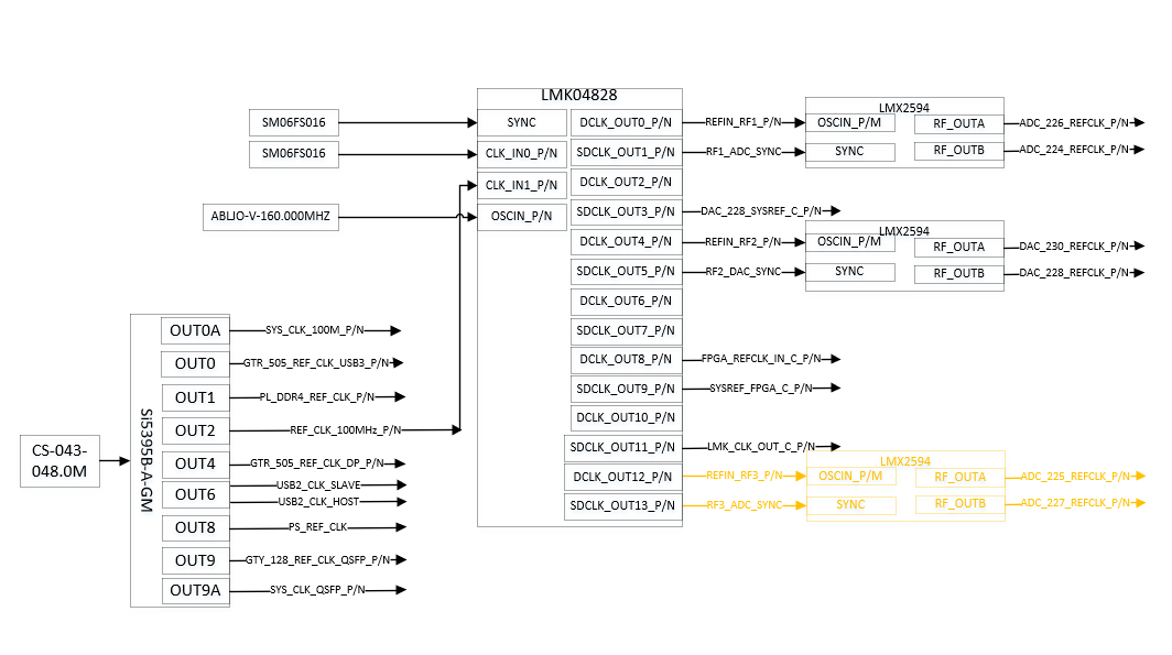
Figure 2.16.2-Clock Distribution Connection Diagram
2.17 Power Supply
The AXW48 uses a 12 V power input. The 12 V system power is converted into different voltages by buck regulators to drive the FPGA and other circuits on the board. The power for the board's ADC and DAC is provided by low-voltage linear LDO regulators, which have good power supply rejection (PSRR).
| BANK | Level (V) | Remarks |
| BANK64, 65, 66 | 1.8V | |
| BANK67, 68, 69 | 1.2V | DDR4 |
| BANK84, 87 | 2.844V | |
| BANK87, 89 | 3.3V | HD BANK |
| BANK128, 129, 130, 131 | 1.2V | QSFP |
| BANK500 | 3.3V | SD, OLED |
| BANK501, 502 | 1.8V | BANK501 (Ethernet), BANK502 (USB3.0) |
| BANK503 | 1.8V fixed | Configuration pin output, mode selection, system reset signal |
Table 2.17.1-AXW48 IO BANK Interface Levels
The power design block diagram of the AXW48 is shown below:
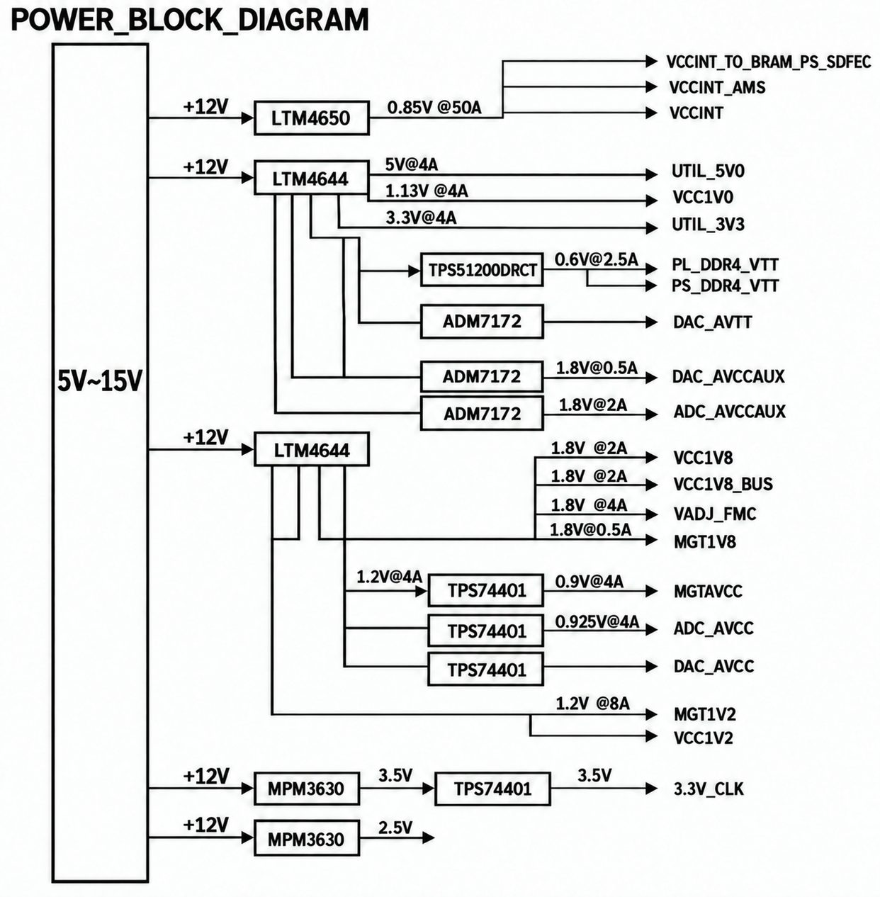
Figure 2.17.1-AXW48 Power Design Block Diagram
2.18 Structure Diagram
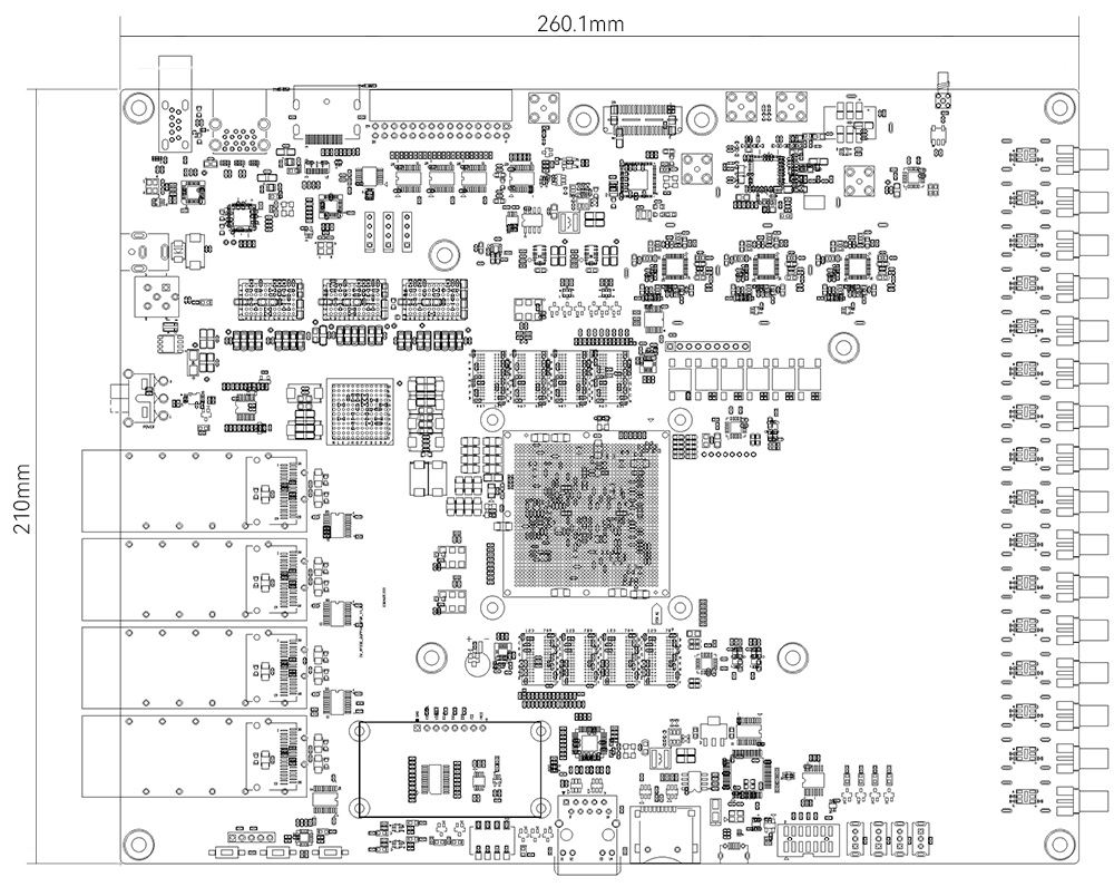
Figure 2.18.1-AXW48 Structure Diagram (Top View)
Appendix: List of Abbreviations
| Abbreviation | Full English Name | Description |
| PS | Processor System | The processing subsystem in an SoC, typically including CPU cores, memory controllers, and peripheral interfaces for running software and operating systems. |
| PL | Programmable Logic | User-configurable FPGA logic resources used to implement custom digital circuits, interface controllers, and hardware acceleration functions. |
| SOC | System on Chip | An integrated circuit that combines processors, memory controllers, peripheral interfaces, and other system functions on a single chip. |
| DDR3 | Double Data Rate 3 SDRAM | A third-generation synchronous dynamic memory technology that transfers data on both edges of the clock signal and is commonly used as system memory. |
| eMMC | Embedded Multi Media Card | An embedded non-volatile storage device that integrates NAND Flash memory and a storage controller in a single package. |
| QSPI | Quad Serial Peripheral Interface | A high-speed serial interface that uses four data lines and is commonly used to connect NOR Flash devices for boot or configuration storage. |
| GTP | Gigabit Transceiver | A high-speed serial transceiver integrated in an FPGA for transmitting and receiving data at multi-gigabit rates. |
| UART | Universal Asynchronous Receiver/Transmitter | An asynchronous serial communication interface that transmits and receives data through TX and RX signal lines. |
| HDMI | High-Definition Multimedia Interface | A digital multimedia interface used to transmit high-definition video and audio signals between source and display devices. |
| PCIe | Peripheral Component Interconnect Express | A high-speed serial expansion bus standard used for communication between processors and devices such as FPGAs, GPUs, and SSDs. |
| USB | Universal Serial Bus | A standard serial interface used for data communication, peripheral connection, and power delivery between electronic devices. |
| JTAG | Joint Test Action Group | A standardized interface used for device testing, boundary scan, FPGA programming, and processor or system debugging. |
| SFP | Small Form-factor Pluggable | A compact, hot-pluggable transceiver interface used for optical or electrical network communication. |
| MIO | Multiplexed I/O | Multiplexed processor I/O pins in an SoC that can be configured for functions such as UART, I2C, SPI, or GPIO. |
| GPHY | Gigabit Ethernet PHY | A Gigabit Ethernet physical-layer transceiver that converts digital Ethernet data into electrical signals for transmission over a physical network medium. |
| I2C | Inter-Integrated Circuit | A two-wire serial communication bus using SDA and SCL lines, commonly used to connect sensors, EEPROMs, and peripheral devices. |
| RGMII | Reduced Gigabit Media Independent Interface | A reduced-pin-count interface between an Ethernet MAC and PHY that supports 10, 100, and 1000 Mbps Ethernet communication. |
| RMII | Reduced Media Independent Interface | A reduced-pin-count interface between an Ethernet MAC and PHY, mainly used for 10 and 100 Mbps Ethernet communication. |
| LED | Light Emitting Diode | A semiconductor device that emits light when electrically driven and is commonly used for power, status, and fault indication. |
| LVDS | Low-Voltage Differential Signaling | A high-speed differential signaling standard that provides low power consumption, low noise, and strong resistance to electromagnetic interference. |
Contact information
Alinx Electronic Limited
Company Website: www.en.alinx.com
Service Hotline: +86 21 67676997
Technical Support:technical@alinx.com