
Appearance
PI-AR035-F1-1 User Manual

Alinx Electronic Limited
Company Website: www.en.alinx.com
Service Hotline: +86 21 67676997
Technical Support : technical@alinx.com
Document Information
| Item | Content |
| Document Name | User Manual |
| Product Model | PI-AR035-F1-1 |
| Document Version | V1.0 |
| Prepared by | Alinx Electronic Limited |
| Release Date | 2026.11.12 |
Document Revision History
| Version | Date | Section | Revision Summary |
| V1.0 | 2026.11.12 | All | Initial Release |
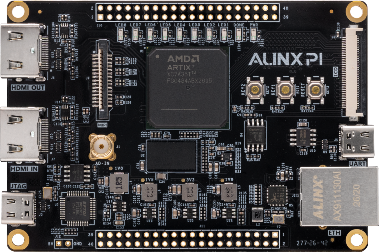
The PI-AR035-F1-1 is an FPGA development platform based on the Xilinx ARTIX-7 series. The board provides one Gigabit Ethernet port, one HDMI input, one HDMI output, one SD card slot, one USB UART port, one EEPROM, one LCD interface, one AD input, one MIPI interface, a TYPE-C download interface and two 40-pin expansion connectors. It is intended for early-stage functional validation of high-speed data transmission, video processing and industrial control applications.
Chapter 1 Introduction
The board uses a Xilinx ARTIX-7 series FPGA, model XC7A35T-2FGG484I, in a 484-pin FBGA package. The FPGA connects to one 2Gbit (256MB) DDR3 SDRAM device, which provides high-speed data read and write between the FPGA and the DDR3 memory. The data width is 16 bits and the read/write clock frequency is 400MHz, giving a system bandwidth of up to 12.8Gbit/s (800Mbps × 16bit) that meets the data buffer requirements of data processing. One 128Mbit QSPI FLASH serves as the FPGA configuration device and stores the configuration file and user data.
The board provides a comprehensive set of peripheral interfaces, including one HDMI output, one HDMI input, one Gigabit Ethernet port, one LCD interface, one MIPI interface, one USB UART port, one SD card interface, one ADC interface and two 40-pin expansion connectors, together with button, LED and EEPROM circuits.
The figure below shows the architecture of the complete development system:
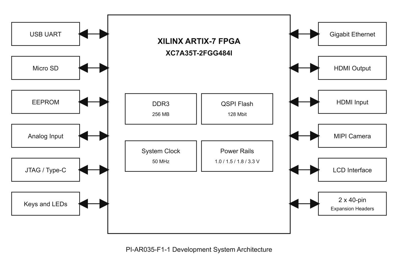
The interfaces and functions implemented on this platform are as follows:
Xilinx ARTIX-7 series FPGA XC7A35T-2FGG484I;
One 2Gbit (256MB) high-speed DDR3 SDRAM, used as data cache for the FPGA;
One 128Mbit QSPI FLASH, used to store the FPGA configuration file and user data;
One 50MHz active crystal oscillator, providing a stable clock source for the FPGA system;
One 10/100/1000Mbps Ethernet RJ-45 interface based on the JLSemi JL2121 industrial-grade GPHY chip, supporting 10/100/1000Mbps transfer rates, full duplex and auto-negotiation.
One HDMI video output interface, supporting up to 1080P@60Hz and multiple output data formats.
One HDMI video input interface, supporting up to 720P@60Hz and multiple input data formats.
One TYPE-C interface, used to power the board and to debug and download the FPGA through the onboard JTAG circuit;
One USB UART interface for communication with a PC, which simplifies debugging; the UART chip is the WCH CH340N and the USB connector is TYPE-C.
One Micro SD card slot, supporting SD and SPI modes;
One AD input interface with an SMA connector, capable of acquiring 0V to 10V analog signals;
Two 40-pin expansion connectors (2.54mm pitch) for connecting dual-camera modules, TFT LCD panels and high-speed AD modules; each connector provides one 5V power pin, two 3.3V power pins, three ground pins and 34 bidirectional IOs.
One MIPI interface (15-pin FPC) for connecting MIPI camera modules;
One LCD interface (40-pin FPC) for connecting the AN-LCD430 4.3-inch TFT module;
Buttons and LEDs: one reset button and two user buttons; one power indicator, one DONE configuration indicator and eight user LEDs.
Chapter 2 Structure and Dimensions
The board measures 100mm×70mm and uses an 8-layer PCB. Four screw mounting holes with a diameter of 3.5mm are provided around the board, and a DXF mechanical drawing is supplied with the board.
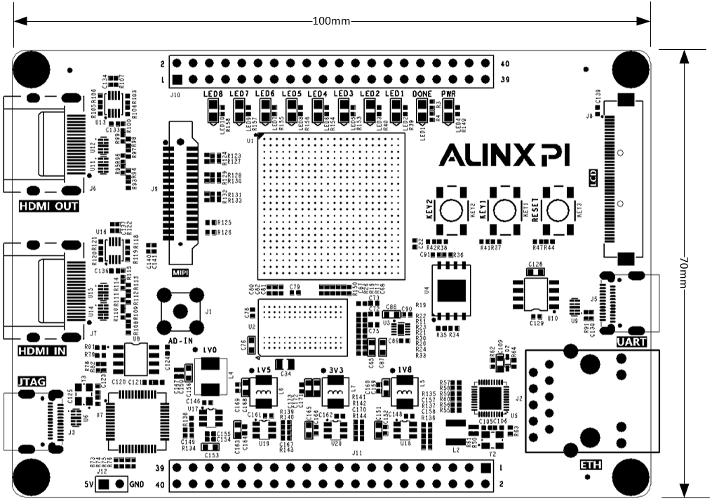
Figure 2.1.1 - Structure Dimension Drawing
Chapter 3 Power Supply
Power input: the board is powered from 5V, either directly through the TYPE-C interface or from an external DC 5V supply. The power input section of the schematic is shown in Figure 3.1.1:
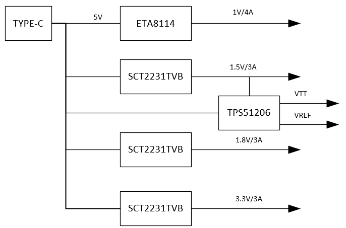
Figure 3.1.1 - Power Input Section of the Schematic
The board is powered from +5V, which four DC/DC converters convert to +3.3V, +1.5V, +1.8V and +1.0V. Three of the outputs deliver up to 3A, and the core supply delivers up to 4A. The VTT and VREF voltages required by the DDR3 memory are generated from 1.5V by the TI TPS51206. Table 3.1.1 lists the function of each supply:
| Power Supply | Function |
| +3.3V | VCCIO of the ARTIX-7, Ethernet, JTAG, HDMI, NOR Flash, EEPROM and SD card |
| +1.8V | Auxiliary supply VCCAUX and VCCBATT of the ARTIX-7, and ADC supply VCCADC |
| +1.0V | Core supply VCCINT and VCCBRAM of the ARTIX-7 |
| +1.5V | DDR3 and BANK34 of the ARTIX-7 |
| VREF, VTT | DDR3 |
Table 3.1.1 - Power Supplies and Functions
The ARTIX-7 FPGA requires a specific power-up sequence, which the circuit design follows: 1.0V → 1.8V → 1.5V → 3.3V.
The PCB uses an 8-layer stack-up with dedicated power and GND planes to ensure power integrity. Test points are provided for each supply rail so that users can measure and verify the voltages.
Chapter 4 ARTIX-7
The board uses a Xilinx ARTIX-7 series FPGA, model XC7A35T-2FGG484I, with speed grade -2, industrial temperature grade and an FGG484 package with 484 pins. The Xilinx ARTIX-7 FPGA part numbering rule is shown in Figure 4.1.1.
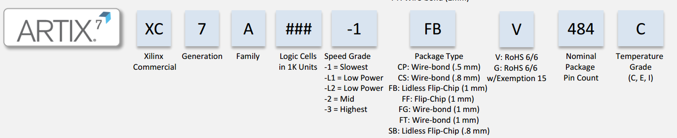
Figure 4.1.1 - FPGA Part Numbering Rule
The main parameters of the XC7A35T are listed in Table 4.1.1.
| Parameter | Specification |
| Logic cells | 33,280 |
| Look-up tables (Slices) | 5,200 |
| Flip-flops (CLB flip-flops) | 41,600 |
| Block RAM (kb) | 1,800 |
| DSP slices | 90 |
| Speed grade | -2 |
| Temperature grade | Industrial |
Table 4.1.1 - Main Parameters of the XC7A35T
4.1 FPGA Power Supply System
The ARTIX-7 FPGA is supplied with VCCINT, VCCBRAM, VCCAUX, VCCO, VMGTAVCC and VMGTAVTT. VCCINT powers the FPGA core and is connected to 1.0V; VCCBRAM powers the Block RAM and is connected to 1.0V; VCCAUX is the auxiliary supply and is connected to 1.8V; VCCO sets the IO voltage of each BANK, including BANK0, BANK14 to BANK16 and BANK34 to BANK35. On the PI-AR035-F1-1, BANK34 drives the DDR3 memory and its VCCO is 1.5V, while the other BANKs use 3.3V; the VCCO of BANK16 can be selected by resistor. The board does not use the GTP transceivers, so no GTP supply is provided.
The ARTIX-7 FPGA requires the following power-up order: VCCINT first, then VCCBRAM, then VCCAUX and finally VCCO. If VCCINT and VCCBRAM share the same voltage, they can be powered up simultaneously. The power-down order is the reverse.
4.2 Clock Configuration
The board uses a SiTime 50MHz active crystal oscillator as the FPGA system clock source. The oscillator output is connected to the FPGA global clock pin (GCLK, Y18), and this clock can drive the user logic inside the FPGA. Users can configure the internal PLL and MMCM to obtain higher clock frequencies. The clock pin assignment is listed in Table 4.2.1.
| FPGA Pin Name | FPGA Pin Number |
| IO_L13P_T2_MRCC_14 | Y18 |
Table 4.2.1 - System Clock Source
Chapter 5 System Peripherals
5.1 DDR3 DRAM
The PI-AR035-F1-1 carries one Samsung 2Gbit (256MB) DDR3 device, model K4B2G1646F-BYMA. The data width is 16 bits and the maximum clock frequency is 400MHz (800Mbps data rate). This DDR3 memory system is connected to the memory interface of FPGA BANK34. The DDR3 SDRAM configuration is listed in Table 5.1.1.
| Designator | Part Number | Capacity | Manufacturer |
| U2 | K4B2G1646F-BYMA | 128M x 16bit | Samsung |
Table 5.1.1 - DDR3 SDRAM Configuration
Signal integrity is a key concern in the DDR3 hardware design. Termination resistors, trace impedance control and length matching were completed during schematic and PCB design to ensure stable high-speed operation of the DDR3 memory. The hardware connection of the DDR3 DRAM is shown in Figure 5.1.1:
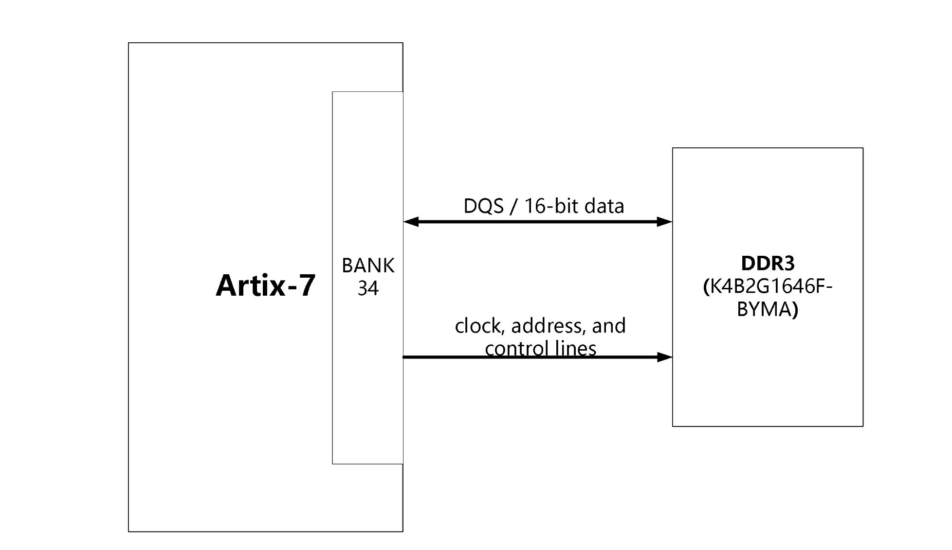
Figure 5.1.1 - DDR3 DRAM Connection Diagram
DDR3 DRAM pin assignment:
| Signal Name | FPGA Pin Name | FPGA Pin Number |
| DDR3_LDQS_P | IO_L9P_T1_DQS_34 | Y3 |
| DDR3_LDQS_N | IO_L9N_T1_DQS_34 | AA3 |
| DDR3_UDQS_P | IO_L3P_T0_DQS_34 | R3 |
| DDR3_UDQS_N | IO_L3N_T0_DQS_34 | R2 |
| DDR3_DQ[0] | IO_L11N_T1_SRCC_34 | AA4 |
| DDR3_DQ [1] | IO_L8N_T1_34 | AB2 |
| DDR3_DQ [2] | IO_L12P_T1_MRCC_34 | V4 |
| DDR3_DQ [3] | IO_L7P_T1_34 | AA1 |
| DDR3_DQ [4] | IO_L8P_T1_34 | AB3 |
| DDR3_DQ [5] | IO_L10N_T1_34 | AB5 |
| DDR3_DQ [6] | IO_L11P_T1_SRCC_34 | Y4 |
| DDR3_DQ [7] | IO_L10P_T1_34 | AA5 |
| DDR3_DQ [8] | IO_L6P_T0_34 | U3 |
| DDR3_DQ [9] | IO_L5P_T0_34 | W1 |
| DDR3_DQ [10] | IO_L2P_T0_34 | U2 |
| DDR3_DQ [11] | IO_L1N_T0_34 | U1 |
| DDR3_DQ [12] | IO_L4N_T0_34 | Y2 |
| DDR3_DQ [13] | IO_L1P_T0_34 | T1 |
| DDR3_DQ [14] | IO_L2N_T0_34 | V2 |
| DDR3_DQ [15] | IO_L5N_T0_34 | Y1 |
| DDR3_LDM | IO_L7N_T1_34 | AB1 |
| DDR3_UDM | IO_L4P_T0_34 | W2 |
| DDR3_A[0] | IO_L22N_T3_34 | AB8 |
| DDR3_A[1] | IO_L16N_T2_34 | V5 |
| DDR3_A[2] | IO_L23N_T3_34 | Y7 |
| DDR3_A[3] | IO_L17P_T2_34 | R6 |
| DDR3_A[4] | IO_L19N_T3_VREF_34 | W7 |
| DDR3_A[5] | IO_25_34 | U7 |
| DDR3_A[6] | IO_L16P_T2_34 | U6 |
| DDR3_A[7] | IO_L19P_T3_34 | V7 |
| DDR3_A[8] | IO_L17N_T2_34 | T6 |
| DDR3_A[9] | IO_L23P_T3_34 | Y8 |
| DDR3_A[10] | IO_L14P_T2_SRCC_34 | T5 |
| DDR3_A[11] | IO_L13P_T2_MRCC_34 | R4 |
| DDR3_A[12] | IO_L13N_T2_MRCC_34 | T4 |
| DDR3_A[13] | IO_L15N_T2_DQS_34 | W5 |
| DDR3_BA[0] | IO_L24P_T3_34 | W9 |
| DDR3_BA[1] | IO_L15P_T2_DQS_34 | W6 |
| DDR3_BA[2] | IO_L22P_T3_34 | AA8 |
| DDR3_S0 | IO_L24N_T3_34 | Y9 |
| DDR3_RAS | IO_L18N_T2_34 | AA6 |
| DDR3_CAS | IO_L20N_T3_34 | AB6 |
| DDR3_WE | IO_L20P_T3_34 | AB7 |
| DDR3_ODT | IO_L18P_T2_34 | Y6 |
| DDR3_RESET | IO_0_34 | T3 |
| DDR3_CLK_P | IO_L21P_T3_DQS_34 | V9 |
| DDR3_CLK_N | IO_L21N_T3_DQS_34 | V8 |
| DDR3_CKE | IO_L14N_T2_SRCC_34 | U5 |
Table 5.1.2 - DDR3 SDRAM Pin Assignment
5.2 QSPI Flash
The board carries one 128Mbit QSPI FLASH device, model GD25Q128ESIGR, which operates at 3.3V (CMOS level). Because Flash memory is non-volatile, the QSPI FLASH can hold the boot image of the FPGA system, which typically contains the FPGA bit file, the soft-core application code and user data files. The model and parameters of the QSPI FLASH are listed in Table 5.2.1.
| Designator | Part Number | Capacity | Manufacturer |
| U4 | GD25Q128ESIGR | 128Mbit | GigaDevice |
Table 5.2.1 - QSPI Flash Model and Parameters
The QSPI FLASH is connected to dedicated pins of FPGA BANK0 and BANK14. The clock is connected to CCLK0 of BANK0, and the data and chip-select signals are connected to D00 to D03 and FCS of BANK14 respectively. Figure 5.2.1 shows the hardware connection of the QSPI Flash.
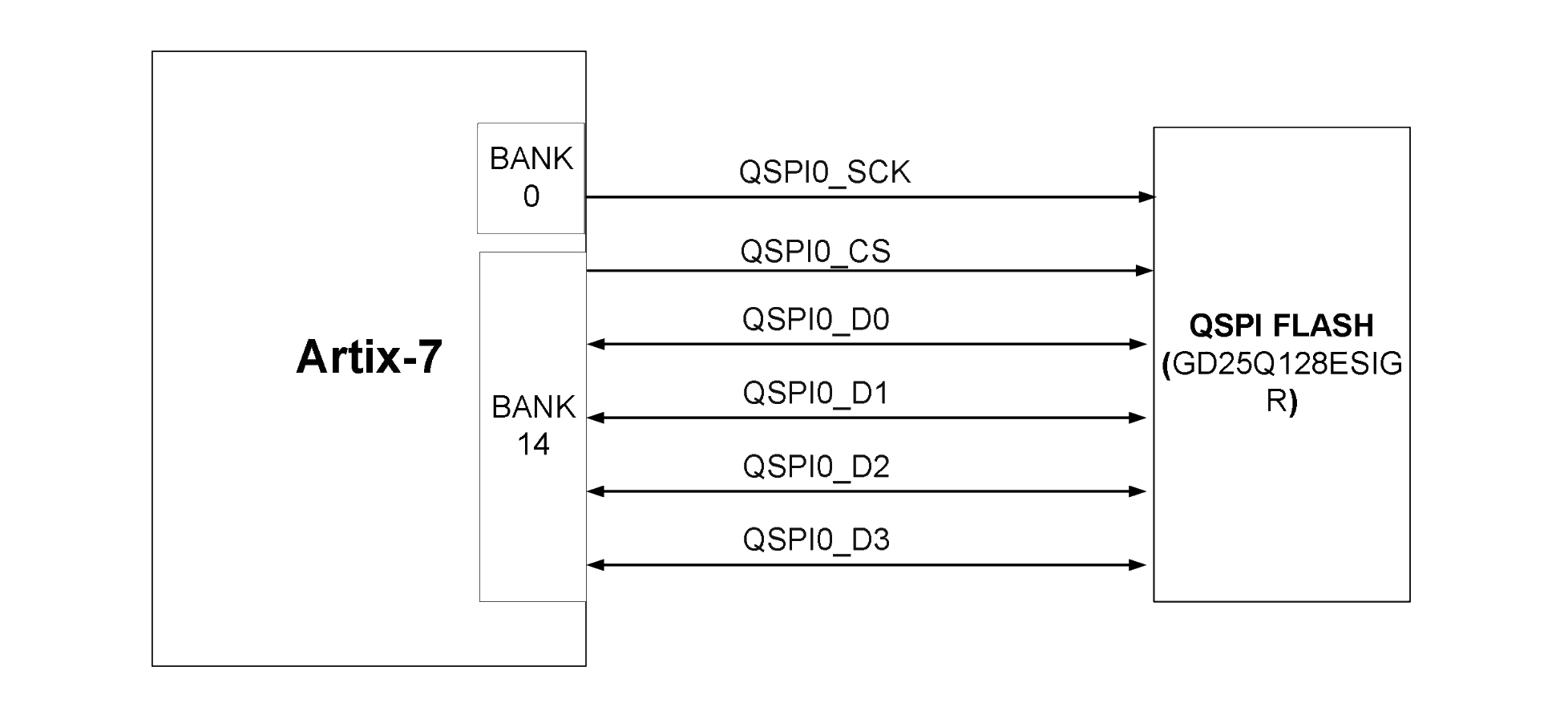
Figure 5.2.1 - QSPI Flash Connection Diagram
Configuration device pin assignment:
| Signal Name | FPGA Pin Name | FPGA Pin Number |
| QSPI_CLK | CCLK_0 | L12 |
| QSPI_CS | IO_L6P_T0_FCS_B_14 | T19 |
| QSPI_D0 | IO_L1P_T0_D00_MOSI_14 | P22 |
| QSPI_D1 | IO_L1N_T0_D01_DIN_14 | R22 |
| QSPI_D2 | IO_L2P_T0_D02_14 | P21 |
| QSPI_D3 | IO_L2N_T0_D03_14 | R21 |
Table 5.2.2 - QSPI Flash Pin Assignment
5.3 Gigabit Ethernet Interface
The PI-AR035-F1-1 uses a JLSemi JL2121-N040I Ethernet PHY to provide network connectivity. The Ethernet PHY is connected to the IO of the ARTIX-7 FPGA. The JL2121-N040I supports 10/100/1000Mbps transfer rates and communicates with the FPGA over an RGMII interface. It supports MDI/MDX auto-crossover, rate auto-negotiation and master/slave auto-negotiation, and its registers can be managed over the MDIO bus.
When the JL2121 is powered up, it samples the level of specific IOs to determine its operating mode. Table 5.3.1 lists the default configuration of the GPHY after power-up.
| Configuration Pin | Description | Configuration Value |
| RXD3_ADR0 RXC_ADR1 RXCTL_ADR2 | PHY address in MDIO/MDC mode | PHY address 001 |
| RXD1_TXDLY | 2 ns delay on the TX clock | Delay |
| RXD0_RXDLY | 2 ns delay on the RX clock | Delay |
Table 5.3.1 - Default Configuration of the PHY Chip
At Gigabit rate, the FPGA and the JL2121 communicate over the RGMII bus at a clock frequency of 125MHz, and data is sampled on both the rising and falling edges of the clock.
At 100Mbps rate, the FPGA and the JL2121 communicate over the RGMII bus at a clock frequency of 25MHz, and data is sampled on both edges of the clock. The connection between the FPGA and the Ethernet PHY is shown in Figure 5.3.1:
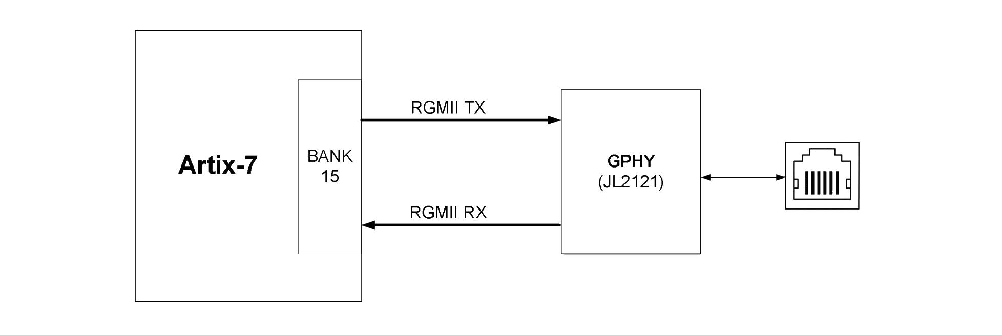
Figure 5.3.1 - FPGA and PHY Connection Diagram
The FPGA pin assignment of the Ethernet PHY is as follows:
| Signal Name | FPGA Pin Name | FPGA Pin Number | Remark |
| PHY_GTXC | IO_L22P_T3_A17_15 | L14 | RGMII transmit clock |
| PHY_TXD0 | IO_25_15 | M17 | Transmit data bit0 |
| PHY_TXD1 | IO_L18N_T2_A23_15 | M20 | Transmit data bit0 |
| PHY_TXD2 | IO_L18P_T2_A24_15 | N20 | Transmit data bit0 |
| PHY_TXD3 | IO_L20N_T3_A19_15 | L13 | Transmit data bit0 |
| PHY_TXEN | IO_L20P_T3_A20_15 | M13 | Transmit enable signal |
| PHY_RXC | IO_L13P_T2_MRCC_15 | K18 | RGMII receive clock |
| PHY_RXD0 | IO_L19N_T3_A21_VREF_15 | K14 | Receive data bit0 |
| PHY_RXD1 | IO_L24P_T3_RS1_15 | M15 | Receive data bit1 |
| PHY_RXD2 | IO_L21N_T3_DQS_A18_15 | J17 | Receive data bit2 |
| PHY_RXD3 | IO_L24N_T3_RS0_15 | M16 | Receive data bit3 |
| PHY_RXDV | IO_L23P_T3_FOE_B_15 | L16 | Receive data valid signal |
| PHY_MDC | IO_L21P_T3_DQS_15 | K17 | MDIO management clock |
| PHY_MDIO | IO_L23N_T3_FWE_B_15 | K16 | MDIO management data |
| PHY_RESET | IO_L22N_T3_A16_15 | L15 | PHY chip reset |
Table 5.3.2 - Ethernet Pin Assignment
5.4 HDMI Output Interface
HDMI (High-Definition Multimedia Interface) is a high-definition multimedia interface. Connector J6 on the PI-AR035-F1-1 is an HDMI output. The HDMI differential signals and clock are connected directly to differential IOs of FPGA BANK35, and the FPGA performs the serial-to-parallel conversion and encoding/decoding internally to produce the HDMI digital video output, which supports up to 1080P@60Hz.
When the board acts as an HDMI source (HDMI OUT), it must supply +5V to the HDMI display device and read its EDID information over the I2C bus. The FPGA IO level is 3.3V while the HDMI side is +5V, so level translation is provided by the UM3202V. The pin assignment of the HDMI output interface is listed in Table 5.4.1:
| Signal Name | FPGA Pin Name | FPGA Pin Number | Remark |
| HDMI1_CLK_P | IO_L3P_T0_DQS_AD5P_35 | E1 | HDMI clock positive |
| HDMI1_CLK_N | IO_L3N_T0_DQS_AD5N_35 | D1 | HDMI clock negative |
| HDMI1_D0_P | IO_L5P_T0_AD13P_35 | G1 | HDMI data 0 positive |
| HDMI1_D0_N | IO_L5N_T0_AD13N_35 | F1 | HDMI data 0 negative |
| HDMI1_D1_P | IO_L7P_T1_AD6P_35 | K1 | HDMI data 1 positive |
| HDMI1_D1_N | IO_L7N_T1_AD6N_35 | J1 | HDMI data 1 negative |
| HDMI1_D2_P | IO_L15P_T2_DQS_35 | M1 | HDMI data 2 positive |
| HDMI1_D2_N | IO_L15N_T2_DQS_35 | L1 | HDMI data 2 negative |
| HDMI1_SCL | IO_L21N_T3_DQS_35 | P4 | HDMI I2C clock |
| HDMI1_SDA | IO_L19N_T3_VREF_35 | N3 | HDMI I2C data |
Table 5.4.1 - HDMI Output Interface Pin Assignment
5.5 HDMI Input Interface
The connector J7 on the PI-AR035-F1-1 is an HDMI input. The HDMI differential signals and clock are connected directly to differential IOs of FPGA BANK35, and the FPGA performs the serial-to-parallel conversion and decoding internally to receive the HDMI digital video input, which supports up to 720P@60Hz.
The HDMI differential signals are received through the IOs of FPGA BANK35, and ESD protection devices are provided at the connector. When the FPGA acts as an HDMI sink, the source reads the EDID information over the I2C bus. The FPGA IO level is 3.3V while the HDMI side is +5V, so level translation is provided by the UM3202V. The pin assignment of the HDMI input interface is listed in Table 5.5.1:
| Signal Name | FPGA Pin Name | FPGA Pin Number | Remark |
| HDMI2_CLK_P | IO_L13P_T2_MRCC_35 | K4 | HDMI clock positive |
| HDMI2_CLK_N | IO_L13N_T2_MRCC_35 | J4 | HDMI clock negative |
| HDMI2_D0_P | IO_L8P_T1_AD14P_35 | H2 | HDMI data 0 positive |
| HDMI2_D0_N | IO_L8N_T1_AD14N_35 | G2 | HDMI data 0 negative |
| HDMI2_D1_P | IO_L22P_T3_35 | P2 | HDMI data 1 positive |
| HDMI2_D1_N | IO_L22N_T3_35 | N2 | HDMI data 1 negative |
| HDMI2_D2_P | IO_L20P_T3_35 | R1 | HDMI data 2 positive |
| HDMI2_D2_N | IO_L20N_T3_35 | P1 | HDMI data 2 negative |
| HDMI2_SCL | IO_L24N_T3_35 | N5 | HDMI I2C clock |
| HDMI2_SDA | IO_25_35 | L6 | HDMI I2C data |
Table 5.5.1 - HDMI Input Interface Pin Assignment
5.6 SD Card
An SD card (Secure Digital Memory Card) is a flash-based storage card. Its standard is defined and maintained by the SD Association (SDA), and it is now one of the most widely used storage media in consumer digital devices.
The board provides one Micro SD card slot that supports both SD and SPI modes. The schematic is shown in Figure 5.6.1.
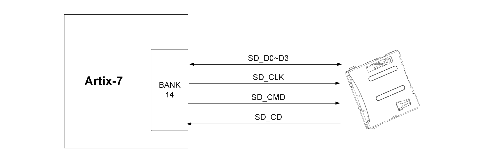
Figure 5.6.1 - SD Card Connection Diagram
SD card pin assignment:
| Signal Name | FPGA Pin Name | FPGA Pin Number | Remark |
| SD_CLK | IO_25_14 | N15 | SD clock signal |
| SD_CMD | IO_L22P_T3_A05_D21_14 | P15 | SD command signal |
| SD_DAT0 | IO_L24P_T3_A01_D17_14 | P16 | SD data DAT0 |
| SD_DAT1 | IO_L24N_T3_A00_D16_14 | R17 | SD data DAT1 |
| SD_DAT2 | IO_L23N_T3_A02_D18_14 | N14 | SD data DAT2 |
| SD_DAT3 | IO_L23P_T3_A03_D19_14 | N13 | SD data DAT3 |
| SD0_CD_N | IO_L22N_T3_A04_D20_14 | R16 | SD card detect signal |
Table 5.6.1 - SD Card Slot Pin Assignment
5.7 USB to UART
The PI-AR035-F1-1 uses a WCH CH340N USB-UART chip with a TYPE-C USB connector. A USB cable connects the board to a USB port of a PC for serial communication. The schematic of the USB UART circuit is shown below:
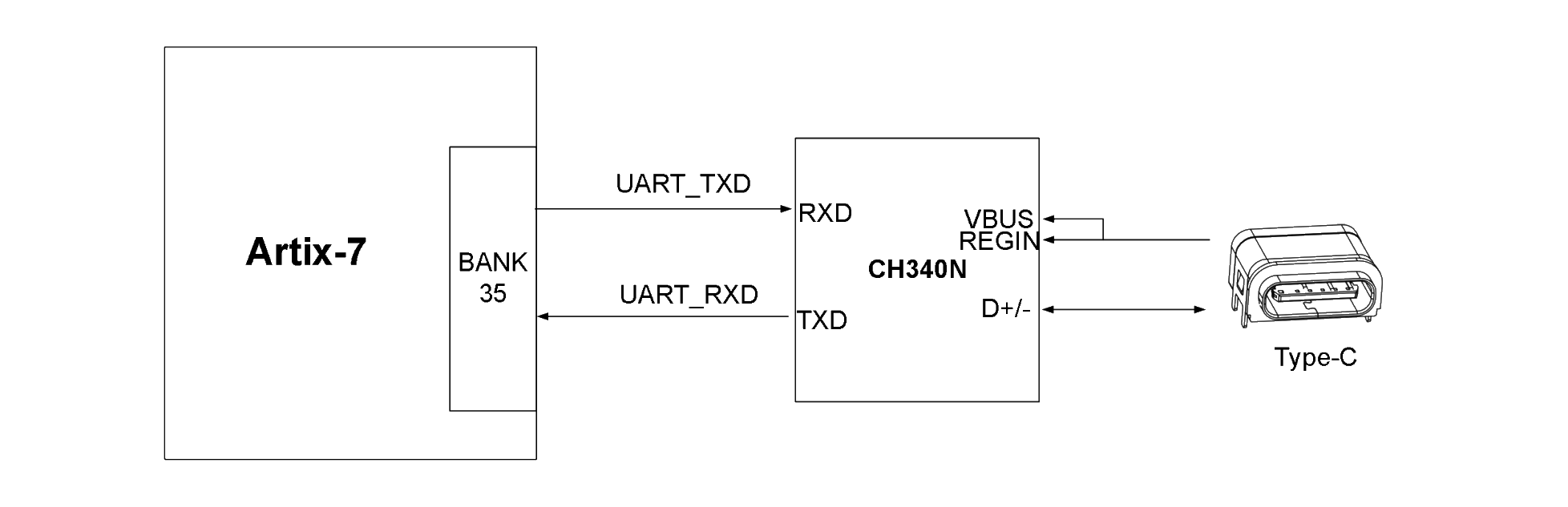
Figure 5.7.1 - UART Connection Diagram
FPGA pin assignment of the USB to UART interface:
| Signal Name | FPGA Pin Name | FPGA Pin Number | Remark |
| UART_TX | IO_L18P_T2_35 | L5 | UART data output |
| UART_RX | IO_L18N_T2_35 | L4 | UART data input |
Table 5.7.1 - UART Pin Assignment
5.8 EEPROM
The PI-AR035-F1-1 carries one EEPROM, model 24LC04, with a capacity of 4Kbit (512 bytes) organized as two 256-byte blocks. It communicates over the I2C bus and is used to demonstrate and verify I2C bus communication. The I2C signals of the EEPROM are connected to the IO of the FPGA. The EEPROM schematic is shown in Figure 5.8.1.
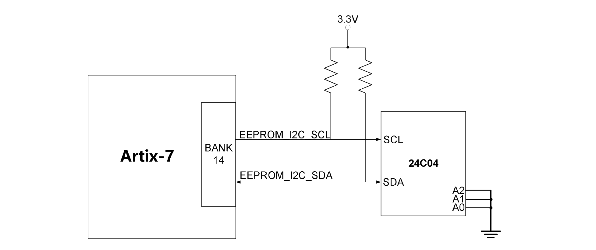
Figure 5.8.1 - EEPROM Connection Diagram
EEPROM pin assignment:
| Signal Name | FPGA Pin Name | FPGA Pin Number |
| EEPROM_I2C_SCL | IO_L13N_T2_MRCC_14 | Y19 |
| EEPROM_I2C_SDA | IO_L6N_T0_D08_VREF_14 | T20 |
Table 5.8.1 - EEPROM Pin Assignment
5.9 LCD Interface
The PI-AR035-F1-1 provides one LCD interface for a 4.3-inch display module. The signals are connected to the IOs of FPGA BANK15. The BANK15 IO pin assignment of the LCD interface is listed in Table 5.9.1:
| Signal Name | FPGA Pin Name | FPGA Pin Number | Remark |
| LCD_R0 | IO_L8N_T1_AD10N_15 | G20 | Bit 0 of LCD red data channel |
| LCD_R1 | IO_L7N_T1_AD2N_15 | H22 | Bit 1 of LCD red data channel |
| LCD_R2 | IO_L11N_T1_SRCC_15 | J21 | Bit 2 of LCD red data channel |
| LCD_R3 | IO_L7P_T1_AD2P_15 | J22 | Bit 3 of LCD red data channel |
| LCD_R4 | IO_L9P_T1_DQS_AD3P_15 | K21 | Bit 4 of LCD red data channel |
| LCD_R5 | IO_L9N_T1_DQS_AD3N_15 | K22 | Bit 5 of LCD red data channel |
| LCD_R6 | IO_L10N_T1_AD11N_15 | L21 | Bit 6 of LCD red data channel |
| LCD_R7 | IO_L15N_T2_DQS_ADV_B_15 | M22 | Bit 7 of LCD red data channel |
| LCD_G0 | IO_L10P_T1_AD11P_15 | M21 | Bit 0 of LCD green data channel |
| LCD_G1 | IO_L15P_T2_DQS_15 | N22 | Bit 1 of LCD green data channel |
| LCD_G2 | IO_L1P_T0_AD0P_15 | H13 | Bit 2 of LCD green data channel |
| LCD_G3 | IO_L6P_T0_15 | H17 | Bit 3 of LCD green data channel |
| LCD_G4 | IO_L8P_T1_AD10P_15 | H20 | Bit 4 of LCD green data channel |
| LCD_G5 | IO_L12N_T1_MRCC_15 | H19 | Bit 5 of LCD green data channel |
| LCD_G6 | IO_L6N_T0_VREF_15 | H18 | Bit 6 of LCD green data channel |
| LCD_G7 | IO_L11P_T1_SRCC_15 | J20 | Bit 7 of LCD green data channel |
| LCD_B0 | IO_L12P_T1_MRCC_15 | J19 | Bit 0 of LCD blue data channel |
| LCD_B1 | IO_0_15 | J16 | Bit 1 of LCD blue data channel |
| LCD_B2 | IO_L13N_T2_MRCC_15 | K19 | Bit 2 of LCD blue data channel |
| LCD_B3 | IO_L5P_T0_AD9P_15 | J15 | Bit 3 of LCD blue data channel |
| LCD_B4 | IO_L14N_T2_SRCC_15 | L20 | Bit 4 of LCD blue data channel |
| LCD_B5 | IO_L14P_T2_SRCC_15 | L19 | Bit 5 of LCD blue data channel |
| LCD_B6 | IO_L16N_T2_A27_15 | L18 | Bit 6 of LCD blue data channel |
| LCD_B7 | IO_L3P_T0_DQS_AD1P_15 | J14 | Bit 7 of LCD blue data channel |
| LCD_CLK | IO_L19P_T3_A22_15 | K13 | LCD clock |
| LCD_HSYNC | IO_L16P_T2_A28_15 | M18 | LCD horizontal sync |
| LCD_VSYNC | IO_L17P_T2_A26_15 | N18 | LCD vertical sync |
| LCD_DE | IO_L17N_T2_A25_15 | N19 | LCD data enable |
| LCD_BL | IO_L1N_T0_AD0N_15 | G13 | LCD backlight enable |
| TP_RST | IO_L2P_T0_AD8P_15 | G15 | LCD touch panel reset |
| TP_SDA | IO_L4P_T0_15 | G17 | LCD touch panel I2C data |
| TP_SCL | IO_L4N_T0_15 | G18 | LCD touch panel I2C clock |
| TP_INTR | IO_L3N_T0_DQS_AD1N_15 | H14 | LCD touch panel interrupt |
| RES0 | IO_L2N_T0_AD8N_15 | G16 | Reserved |
| RES1 | IO_L5N_T0_AD9N_15 | H15 | Reserved |
Table 5.9.1 - LCD Pin Assignment
5.10 AD Input Interface
The PI-AR035-F1-1 provides one AD input interface with an SMA connector. It acquires external analog signals and performs AD conversion; the input signal is converted to a differential signal and fed to the FPGA. The schematic of the AD acquisition circuit is shown in Figure 5.10.1:
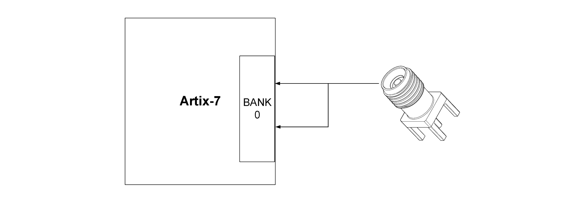
Figure 5.10.1 - AD Acquisition Circuit Diagram
FPGA pin assignment of the AD acquisition circuit:
| Signal Name | FPGA Pin Name | FPGA Pin Number | Remark |
| ADC_P | VP_0 | L10 | AD_IN_P |
| ADC_N | VN_0 | M9 | AD_IN_N |
Table 5.10.1 - FPGA Pin Assignment of the AD Acquisition Circuit
5.11 MIPI Interface
The PI-AR035-F1-1 provides one MIPI camera interface for connecting a MIPI OV5640 camera module. The interface signals are connected to the IOs of FPGA BANK35. The MIPI interface schematic is shown in Figure 5.11.1.
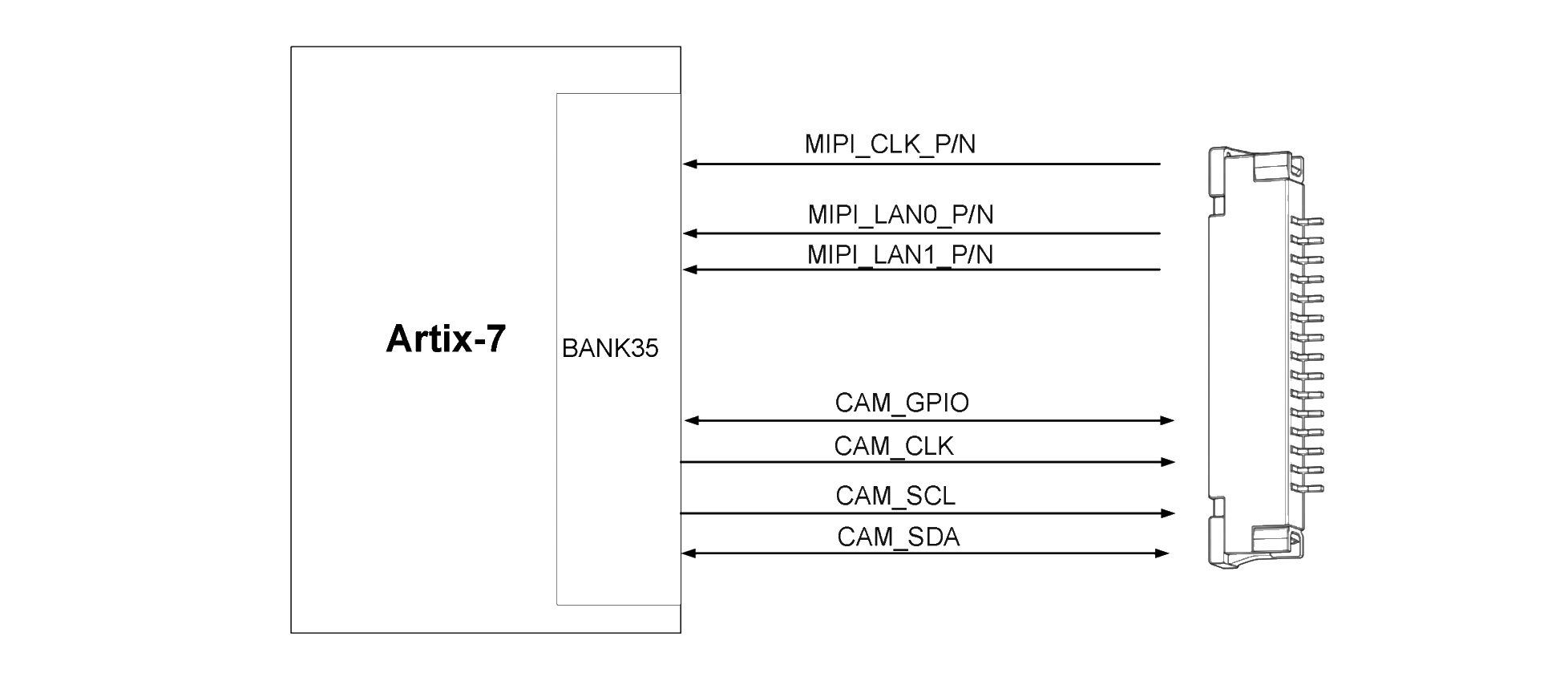
Figure 5.11.1 - MIPI Interface Schematic
MIPI interface pin assignment:
| Signal Name | FPGA Pin Name | FPGA Pin Number | Remark |
| MIPI_CSI_L0_N | IO_L4N_T0_35 | D2 | LANE0 negative in High Speed mode |
| LP_MIPI_CSI_L0_N | IO_L2N_T0_AD12N_35 | B2 | LANE0 negative in Low Power mode |
| LP_MIPI_CSI_L0_P | IO_L2P_T0_AD12P_35 | C2 | LANE0 positive in Low Power mode |
| MIPI_CSI_L0_P | IO_L4P_T0_35 | E2 | LANE0 positive in High Speed mode |
| MIPI_CSI_L1_N | IO_L6N_T0_VREF_35 | E3 | LANE1 negative in High Speed mode |
| LP_MIPI_CSI_L1_N | IO_L9N_T1_DQS_AD7N_35 | J2 | LANE1 negative in Low Power mode |
| LP_MIPI_CSI_L1_P | IO_L9P_T1_DQS_AD7P_35 | K2 | LANE1 positive in Low Power mode |
| MIPI_CSI_L1_P | IO_L6P_T0_35 | F3 | LANE1 positive in High Speed mode |
| MIPI_CSI_C_N | IO_L11N_T1_SRCC_35 | G3 | Clock negative in High Speed mode |
| LP_MIPI_CSI_C_N | IO_L1N_T0_AD4N_35 | A1 | Clock negative in Low Power mode |
| LP_MIPI_CSI_C_P | IO_L1P_T0_AD4P_35 | B1 | Clock positive in Low Power mode |
| MIPI_CSI_C_P | IO_L11P_T1_SRCC_35 | H3 | Clock positive in High Speed mode |
| CAM_GPIO | IO_L16P_T2_35 | M3 | Camera GPIO control |
| CAM_CLK | IO_L17N_T2_35 | J6 | Camera clock input |
| CAM_SCL | IO_L17P_T2_35 | K6 | Camera I2C clock |
| CAM_SDA | IO_L16N_T2_35 | M2 | Camera I2C data |
Table 5.11.1 - MIPI Pin Assignment
5.12 Expansion Connectors J10 and J11
The PI-AR035-F1-1 provides two 40-pin expansion connectors, J10 and J11, with 2.54mm pitch, for connecting expansion modules or user-designed external circuits. The IOs of J10 are connected to FPGA BANK16, and the level standard can be selected by fitting R162 or R163; the IOs of J11 are connected to BANK14 and are fixed at 3.3V.
Each expansion connector carries 40 signals: one 5V power pin (output), two 3.3V power pins (output), three ground pins and 34 bidirectional IOs. In the PCB layout of the expansion connectors, the P/N pairs are routed as differential traces with a controlled differential impedance of 100Ω.
Caution: do not connect the IOs directly to 5V devices, as this may damage the FPGA. A level translator is required when connecting 5V devices.
J10 expansion connector pin assignment:
| J10 Pin | Signal Name | FPGA Pin Name | FPGA Pin Number |
| PIN1 | GND | - | - |
| PIN2 | +5V | - | - |
| PIN3 | EX_IO1_1N | IO_L1N_T0_16 | F14 |
| PIN4 | EX_IO1_1P | IO_L1P_T0_16 | F13 |
| PIN5 | EX_IO1_2N | IO_L4N_T0_16 | E14 |
| PIN6 | EX_IO1_2P | IO_L4P_T0_16 | E13 |
| PIN7 | EX_IO1_3N | IO_L6N_T0_VREF_16 | D15 |
| PIN8 | EX_IO1_3P | IO_L6P_T0_16 | D14 |
| PIN9 | EX_IO1_4N | IO_L8N_T1_16 | B13 |
| PIN10 | EX_IO1_4P | IO_L8P_T1_16 | C13 |
| PIN11 | EX_IO1_5N | IO_L3N_T0_DQS_16 | C15 |
| PIN12 | EX_IO1_5P | IO_L3P_T0_DQS_16 | C14 |
| PIN13 | EX_IO1_6N | IO_L7N_T1_16 | B16 |
| PIN14 | EX_IO1_6P | IO_L7P_T1_16 | B15 |
| PIN15 | EX_IO1_7N | IO_L12N_T1_MRCC_16 | C17 |
| PIN16 | EX_IO1_7P | IO_L12P_T1_MRCC_16 | D17 |
| PIN17 | EX_IO1_8N | IO_L11N_T1_SRCC_16 | B18 |
| PIN18 | EX_IO1_8P | IO_L11P_T1_SRCC_16 | B17 |
| PIN19 | EX_IO1_9N | IO_L13N_T2_MRCC_16 | C19 |
| PIN20 | EX_IO1_9P | IO_L13P_T2_MRCC_16 | C18 |
| PIN21 | EX_IO1_10N | IO_L10N_T1_16 | A14 |
| PIN22 | EX_IO1_10P | IO_L10P_T1_16 | A13 |
| PIN23 | EX_IO1_11N | IO_L9N_T1_DQS_16 | A16 |
| PIN24 | EX_IO1_11P | IO_L9P_T1_DQS_16 | A15 |
| PIN25 | EX_IO1_12N | IO_L17N_T2_16 | A19 |
| PIN26 | EX_IO1_12P | IO_L17P_T2_16 | A18 |
| PIN27 | EX_IO1_13N | IO_L16N_T2_16 | A20 |
| PIN28 | EX_IO1_13P | IO_L16P_T2_16 | B20 |
| PIN29 | EX_IO1_14N | IO_L5N_T0_16 | D16 |
| PIN30 | EX_IO1_14P | IO_L5P_T0_16 | E16 |
| PIN31 | EX_IO1_15N | IO_L14N_T2_SRCC_16 | D19 |
| PIN32 | EX_IO1_15P | IO_L14P_T2_SRCC_16 | E19 |
| PIN33 | EX_IO1_16N | IO_L15N_T2_DQS_16 | E18 |
| PIN34 | EX_IO1_16P | IO_L15P_T2_DQS_16 | F18 |
| PIN35 | EX_IO1_17N | IO_L2N_T0_16 | E17 |
| PIN36 | EX_IO1_17P | IO_L2P_T0_16 | F16 |
| PIN37 | GND | - | - |
| PIN38 | GND | - | - |
| PIN39 | +3.3V | - | - |
| PIN40 | +3.3V | - | - |
Table 5.12.1 - J10 Expansion Connector Pin Assignment
J11 expansion connector pin assignment:
| J11 Pin | Signal Name | FPGA Pin Name | FPGA Pin Number |
| PIN1 | GND | - | - |
| PIN2 | +5V | - | - |
| PIN3 | EX_IO2_1N | IO_L21N_T3_DQS_A06_D22_14 | P17 |
| PIN4 | EX_IO2_1P | IO_L21P_T3_DQS_14 | N17 |
| PIN5 | EX_IO2_2N | IO_L5N_T0_D07_14 | R19 |
| PIN6 | EX_IO2_2P | IO_L5P_T0_D06_14 | P19 |
| PIN7 | EX_IO2_3N | IO_L20N_T3_A07_D23_14 | T18 |
| PIN8 | EX_IO2_3P | IO_L20P_T3_A08_D24_14 | R18 |
| PIN9 | EX_IO2_4N | IO_L4N_T0_D05_14 | U21 |
| PIN10 | EX_IO2_4P | IO_L4P_T0_D04_14 | T21 |
| PIN11 | EX_IO2_5N | IO_L11N_T1_SRCC_14 | V20 |
| PIN12 | EX_IO2_5P | IO_L11P_T1_SRCC_14 | U20 |
| PIN13 | EX_IO2_6N | IO_L18N_T2_A11_D27_14 | U18 |
| PIN14 | EX_IO2_6P | IO_L18P_T2_A12_D28_14 | U17 |
| PIN15 | EX_IO2_7N | IO_L14N_T2_SRCC_14 | V19 |
| PIN16 | EX_IO2_7P | IO_L14P_T2_SRCC_14 | V18 |
| PIN17 | EX_IO2_8N | IO_L3N_T0_DQS_EMCCLK_14 | V22 |
| PIN18 | EX_IO2_8P | IO_L3P_T0_DQS_PUDC_B_14 | U22 |
| PIN19 | EX_IO2_9N | IO_L7N_T1_D10_14 | W22 |
| PIN20 | EX_IO2_9P | IO_L7P_T1_D09_14 | W21 |
| PIN21 | EX_IO2_10N | IO_L9N_T1_DQS_D13_14 | Y22 |
| PIN22 | EX_IO2_10P | IO_L9P_T1_DQS_14 | Y21 |
| PIN23 | EX_IO2_11N | IO_L12N_T1_MRCC_14 | W20 |
| PIN24 | EX_IO2_11P | IO_L12P_T1_MRCC_14 | W19 |
| PIN25 | EX_IO2_12N | IO_L10N_T1_D15_14 | AB22 |
| PIN26 | EX_IO2_12P | IO_L10P_T1_D14_14 | AB21 |
| PIN27 | EX_IO2_13N | IO_L8N_T1_D12_14 | AA21 |
| PIN28 | EX_IO2_13P | IO_L8P_T1_D11_14 | AA20 |
| PIN29 | EX_IO2_14N | IO_L15N_T2_DQS_DOUT_CSO_B_14 | AB20 |
| PIN30 | EX_IO2_14P | IO_L15P_T2_DQS_RDWR_B_14 | AA19 |
| PIN31 | EX_IO2_15N | IO_L17N_T2_A13_D29_14 | AB18 |
| PIN32 | EX_IO2_15P | IO_L17P_T2_A14_D30_14 | AA18 |
| PIN33 | EX_IO2_16N | IO_L16N_T2_A15_D31_14 | W17 |
| PIN34 | EX_IO2_16P | IO_L16P_T2_CSI_B_14 | V17 |
| PIN35 | EX_IO2_17N | IO_L19N_T3_A09_D25_VREF_14 | R14 |
| PIN36 | EX_IO2_17P | IO_L19P_T3_A10_D26_14 | P14 |
| PIN37 | GND | - | - |
| PIN38 | GND | - | - |
| PIN39 | +3.3V | - | - |
| PIN40 | +3.3V | - | - |
Table 5.12.2 - J11 Expansion Connector Pin Assignment
5.13 User Buttons
The PI-AR035-F1-1 provides one reset button RESET and two user buttons KEY1 and KEY2, all connected to general-purpose IOs of the FPGA. The buttons are active low: the IO reads low when the button is pressed and high when it is released. The button circuit is shown in Figure 5.13.1.
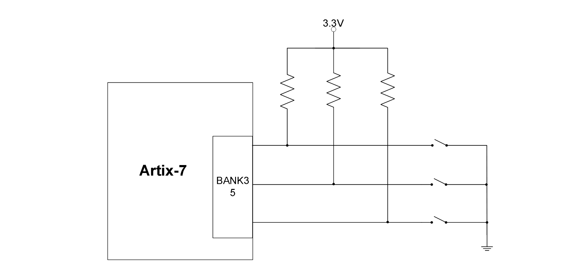
Figure 5.13.1 - Button Hardware Design Diagram
FPGA pin assignment of the buttons:
| Signal Name | FPGA Pin Name | FPGA Pin Number | Remark |
| KEY1 | IO_L14P_T2_SRCC_35 | L3 | KEY1 |
| KEY2 | IO_L14N_T2_SRCC_35 | K3 | KEY2 |
| RESET | IO_L23P_T3_35 | M6 | RESET |
Table 5.13.1 - Button Pin Assignment
5.14 User LEDs
The PI-AR035-F1-1 has ten red LEDs: one power indicator (LED4), one configuration indicator (LED1) and eight user LEDs. After the board is powered up, the power indicator LED4 lights up, and the DONE indicator LED1 lights up once the FPGA is configured. The user LEDs are connected to general-purpose IOs of the FPGA: the LED is on when the IO outputs low and off when the IO outputs high. The hardware connection of the user LEDs is shown in Figure 5.14.1.
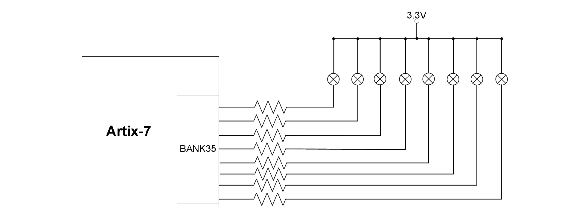
Figure 5.14.1 - LED Hardware Design Diagram
FPGA pin assignment of the LEDs:
| Signal Name | FPGA Pin Name | FPGA Pin Number |
| LED1 | IO_L23N_T3_35 | M5 |
| LED2 | IO_L24P_T3_35 | P6 |
| LED3 | IO_L19P_T3_35 | N4 |
| LED4 | IO_L21P_T3_DQS_35 | P5 |
| LED5 | IO_L10P_T1_AD15P_35 | J5 |
| LED6 | IO_L10N_T1_AD15N_35 | H5 |
| LED7 | IO_L12P_T1_MRCC_35 | H4 |
| LED8 | IO_L12N_T1_MRCC_35 | G4 |
Table 5.14.1 - LED Pin Assignment
Appendix: List of Abbreviations
| Abbreviation | Full English Name | Description |
| PS | Processor System | The processing subsystem in an SoC, typically including CPU cores, memory controllers, and peripheral interfaces for running software and operating systems. |
| PL | Programmable Logic | User-configurable FPGA logic resources used to implement custom digital circuits, interface controllers, and hardware acceleration functions. |
| SOC | System on Chip | An integrated circuit that combines processors, memory controllers, peripheral interfaces, and other system functions on a single chip. |
| DDR3 | Double Data Rate 3 SDRAM | A third-generation synchronous dynamic memory technology that transfers data on both edges of the clock signal and is commonly used as system memory. |
| eMMC | Embedded Multi Media Card | An embedded non-volatile storage device that integrates NAND Flash memory and a storage controller in a single package. |
| QSPI | Quad Serial Peripheral Interface | A high-speed serial interface that uses four data lines and is commonly used to connect NOR Flash devices for boot or configuration storage. |
| GTP | Gigabit Transceiver | A high-speed serial transceiver integrated in an FPGA for transmitting and receiving data at multi-gigabit rates. |
| UART | Universal Asynchronous Receiver/Transmitter | An asynchronous serial communication interface that transmits and receives data through TX and RX signal lines. |
| HDMI | High-Definition Multimedia Interface | A digital multimedia interface used to transmit high-definition video and audio signals between source and display devices. |
| PCIe | Peripheral Component Interconnect Express | A high-speed serial expansion bus standard used for communication between processors and devices such as FPGAs, GPUs, and SSDs. |
| USB | Universal Serial Bus | A standard serial interface used for data communication, peripheral connection, and power delivery between electronic devices. |
| JTAG | Joint Test Action Group | A standardized interface used for device testing, boundary scan, FPGA programming, and processor or system debugging. |
| SFP | Small Form-factor Pluggable | A compact, hot-pluggable transceiver interface used for optical or electrical network communication. |
| MIO | Multiplexed I/O | Multiplexed processor I/O pins in an SoC that can be configured for functions such as UART, I2C, SPI, or GPIO. |
| GPHY | Gigabit Ethernet PHY | A Gigabit Ethernet physical-layer transceiver that converts digital Ethernet data into electrical signals for transmission over a physical network medium. |
| I2C | Inter-Integrated Circuit | A two-wire serial communication bus using SDA and SCL lines, commonly used to connect sensors, EEPROMs, and peripheral devices. |
| RGMII | Reduced Gigabit Media Independent Interface | A reduced-pin-count interface between an Ethernet MAC and PHY that supports 10, 100, and 1000 Mbps Ethernet communication. |
| RMII | Reduced Media Independent Interface | A reduced-pin-count interface between an Ethernet MAC and PHY, mainly used for 10 and 100 Mbps Ethernet communication. |
| LED | Light Emitting Diode | A semiconductor device that emits light when electrically driven and is commonly used for power, status, and fault indication. |
| LVDS | Low-Voltage Differential Signaling | A high-speed differential signaling standard that provides low power consumption, low noise, and strong resistance to electromagnetic interference. |
Contact information
Alinx Electronic Limited
Company Website: www.en.alinx.com
Service Hotline: +86 21 67676997
Technical Support:technical@alinx.com